
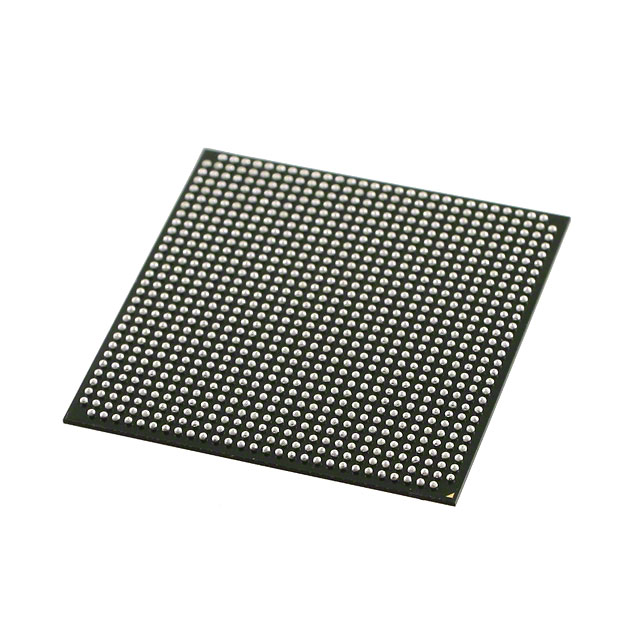
5AGXBA3D6F31C6N
| Part Description |
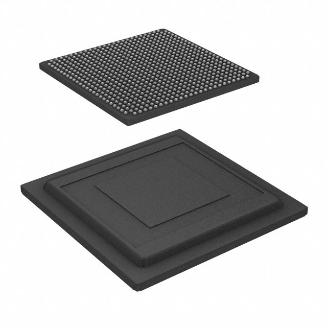
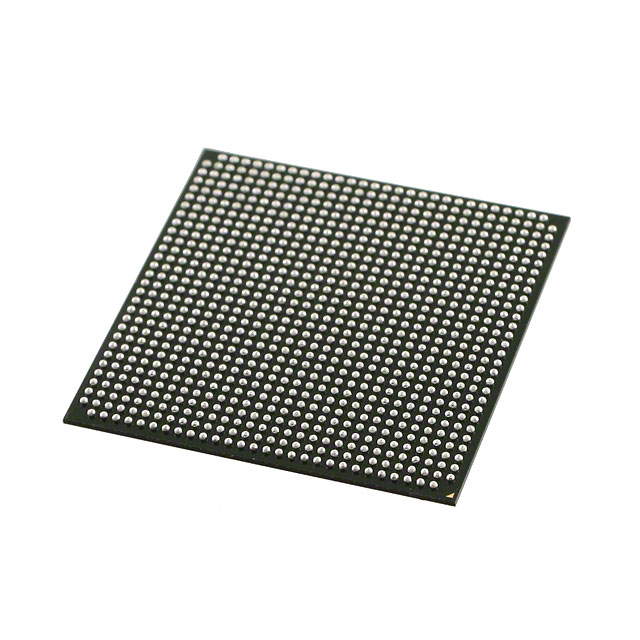
Arria V GX Field Programmable Gate Array (FPGA) IC 416 11746304 156000 896-BBGA, FCBGA |
|---|---|
| Quantity | 1,781 Available (as of October 7, 2026) |
| Product Category | Field Programmable Gate Array (FPGA) |
|---|---|
| Manufacturer | Intel |
| Manufacturing Status | Obsolete |
| Manufacturer Standard Lead Time | Contact Us |
| Datasheet |
Specifications & Environmental
| Device Package | 896-FBGA (31x31) | Grade | Commercial | Operating Temperature | 0°C – 85°C | ||
|---|---|---|---|---|---|---|---|
| Package / Case | 896-BBGA, FCBGA | Number of I/O | 416 | Voltage | 1.07 V - 1.13 V | ||
| Mounting Method | Surface Mount | RoHS Compliance | RoHS Compliant | REACH Compliance | REACH Unknown | ||
| Moisture Sensitivity Level | 3 (168 Hours) | Number of LABs/CLBs | 7362 | Number of Logic Elements/Cells | 156000 | ||
| Number of Gates | N/A | ECCN | 3A001A2C | HTS Code | 8542.39.0001 | ||
| Qualification | N/A | Total RAM Bits | 11746304 |
Overview of 5AGXBA3D6F31C6N – Arria V GX FPGA, 156,000 logic elements, 416 I/Os, 896‑BBGA
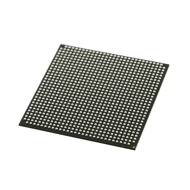
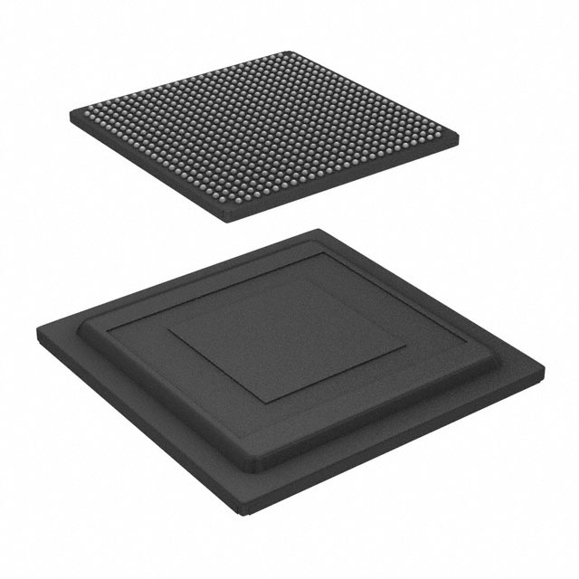
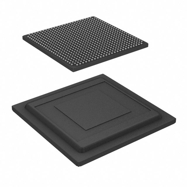
The 5AGXBA3D6F31C6N is an Arria V GX field-programmable gate array (FPGA) IC from Intel, provided in an 896‑BBGA FCBGA package. It delivers a high on-chip resource set including 156,000 logic elements and 11,746,304 bits of embedded RAM, and exposes 416 I/O pins for system interfacing.
Specified for commercial-grade use, the device operates from a core supply range of 1.07 V to 1.13 V and across an ambient temperature range of 0 °C to 85 °C. It is RoHS compliant and is supplied in a 896‑FBGA (31×31) package footprint.
Key Features
- Logic Capacity 156,000 logic elements provide substantial programmable logic resources for complex digital designs and custom datapaths.
- On‑chip Memory 11,746,304 total RAM bits enable large on-chip buffering, state storage, and memory-intensive logic implementations without immediate external memory dependence.
- I/O Count 416 I/O pins support wide external connectivity and flexible interfacing to peripherals and system buses.
- Package 896‑BBGA (FCBGA) package with supplier device package 896‑FBGA (31×31) for compact board-level integration.
- Power Core voltage supply specified from 1.07 V to 1.13 V for predictable power and timing behavior.
- Operating Conditions Commercial grade with an ambient operating temperature range of 0 °C to 85 °C.
- Standards Compliance RoHS compliant for regulatory and environmental considerations.
- Documented Family Support Part of the Arria V device family with comprehensive device datasheet information available for electrical, switching, and configuration specifications.
Typical Applications
- Custom digital acceleration Use the device’s 156,000 logic elements and extensive on‑chip RAM to implement bespoke accelerators and data‑path logic.
- Prototyping and system integration High I/O count and dense logic resources make the device suitable for prototyping system architectures and integrating custom logic into broader designs.
- On‑chip buffering and control Large embedded RAM capacity supports control-state storage, buffering, and local memory needs within complex FPGA designs.
Unique Advantages
- Large programmable fabric 156,000 logic elements offer designers the headroom to implement sizable, multi‑function logic blocks without immediate partitioning across devices.
- Significant on‑chip RAM Over 11.7 million bits of RAM reduce dependence on external memory for many buffering and state‑holding tasks, simplifying board design.
- High I/O density 416 I/Os provide flexible interfacing options for parallel buses, high‑pin-count peripherals, and mixed signal front‑end connectivity.
- Compact BGA footprint 896‑BBGA (31×31) package balances high pin count with a compact board footprint for space-constrained systems.
- Predictable power envelope A defined core supply range (1.07 V–1.13 V) supports consistent power budgeting and thermal planning.
- Commercial availability Commercial grade specification and RoHS compliance facilitate deployment in mainstream electronic products and designs.
Why Choose 5AGXBA3D6F31C6N?
The 5AGXBA3D6F31C6N positions itself as a high‑capacity Arria V GX device for designs that require substantial programmable logic, abundant on‑chip RAM, and a large I/O complement in a compact BGA package. Its documented electrical and configuration specifications in the Arria V family datasheet support system-level planning for power, timing, and configuration.
This part is suited to teams and projects that need dense logic and memory resources within a commercial‑grade FPGA package, enabling integration of custom logic functions, on‑chip buffering, and broad external interfacing while adhering to RoHS environmental requirements.
If you would like pricing information, availability, or to submit a quote request for 5AGXBA3D6F31C6N, please request a quote or submit an inquiry and our team will respond with next steps.





















Date Founded: 1968
Headquarters: Santa Clara, California, USA
Employees: 130,000+
Revenue: $54.23 Billion
Certifications and Memberships: ISO9001:2015, ISO14001:2015, ISO17025:2017, ISO27001:2022, ISO45001:2018, ISO50001:2018


