
5AGXBA3D6F27C6G
| Part Description |
Arria V GX Field Programmable Gate Array (FPGA) IC 336 11746304 156000 672-BBGA, FCBGA |
|---|---|
| Quantity | 721 Available (as of June 15, 2026) |

| Product Category | Field Programmable Gate Array (FPGA) |
|---|---|
| Manufacturer | Intel |
| Manufacturing Status | Active |
| Manufacturer Standard Lead Time | 16 Weeks |
| Datasheet |
Specifications & Environmental
| Device Package | 672-FBGA (27x27) | Grade | Commercial | Operating Temperature | 0°C – 85°C | ||
|---|---|---|---|---|---|---|---|
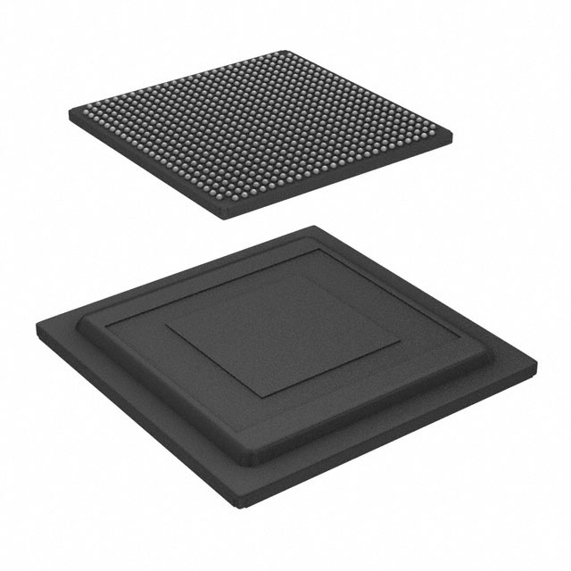
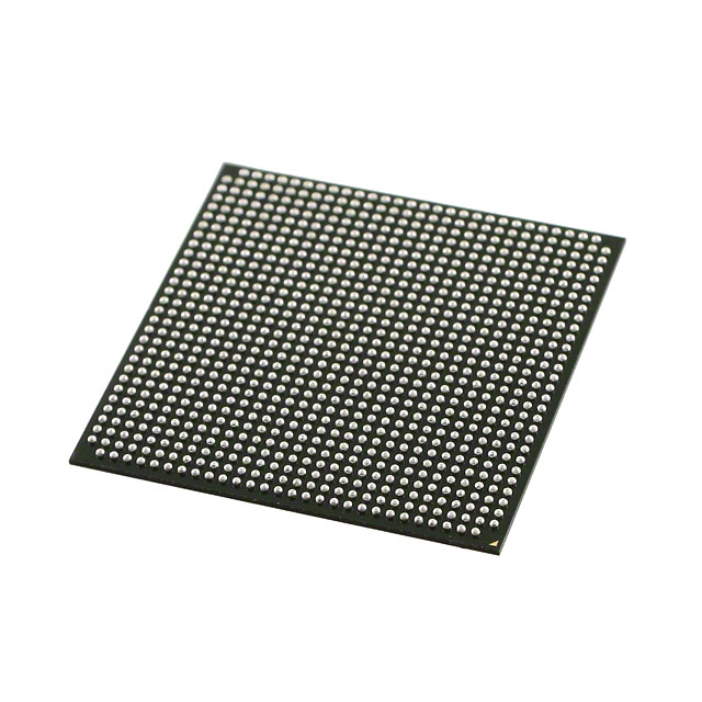
| Package / Case | 672-BBGA, FCBGA | Number of I/O | 336 | Voltage | 1.07 V - 1.13 V | ||
| Mounting Method | Surface Mount | RoHS Compliance | RoHS Compliant | REACH Compliance | REACH Unaffected | ||
| Moisture Sensitivity Level | 3 (168 Hours) | Number of LABs/CLBs | 7362 | Number of Logic Elements/Cells | 156000 | ||
| Number of Gates | N/A | ECCN | PENDING ECCN | HTS Code | 0000.00.0000 | ||
| Qualification | N/A | Total RAM Bits | 11746304 |
Overview of 5AGXBA3D6F27C6G – Arria V GX Field Programmable Gate Array (FPGA) – 156,000 logic elements, 672-FBGA (27×27)
The 5AGXBA3D6F27C6G is an Intel Arria V GX commercial-grade Field Programmable Gate Array (FPGA) supplied in a 672-ball FCBGA package. It provides a large programmable fabric with defined on-chip memory and I/O capability for commercial embedded and system designs that require configurable logic and memory resources.
Key values of this device stem from its logic capacity, on-chip RAM, and a high-pin-count package that supports dense I/O integration while operating within a 1.07 V to 1.13 V core supply range and a 0 °C to 85 °C operating temperature window.
Key Features
- Logic Capacity 156,000 logic elements provide significant programmable logic resources for implementing complex digital functions and custom accelerators.
- Logic Blocks 7,362 logic blocks (device grouping metric) for organizing and mapping logic structures across the fabric.
- On‑Chip Memory 11,746,304 total RAM bits of embedded memory enable local data buffering, FIFOs, and distributed storage without immediate reliance on external memory.
- I/O Density 336 device I/O pins accommodate broad peripheral interfacing and high-channel count connectivity in compact board designs.
- Package and Mounting 672-BBGA FCBGA (supplier package: 672-FBGA, 27×27) in a surface-mount format to support high-density board layouts.
- Power Range Core voltage supply specified at 1.07 V to 1.13 V, enabling predictable power budgeting in system designs.
- Commercial Grade Rated for commercial operating conditions with an ambient temperature range of 0 °C to 85 °C.
Typical Applications
- Commercial programmable systems Use the device to implement custom logic, protocol bridging, and control functions in commercial electronics that operate within specified temperature and voltage ranges.
- High‑density I/O subsystems Leverage 336 I/O pins and the 672‑ball FCBGA package to integrate multiple interfaces and peripherals on compact PCBs.
- On‑chip buffering and control Use the 11,746,304 bits of embedded RAM for local buffering, packet queues, or temporary data storage within an FPGA-based control path.
Unique Advantages
- Substantial programmable fabric: 156,000 logic elements provide the headroom to implement large-scale custom logic and partition designs across the device.
- Integrated RAM capacity: 11.7 Mb of on-chip RAM reduces dependence on external memory for many buffering and state-storage needs, simplifying board-level memory requirements.
- High I/O count in a compact package: 336 I/O pins in a 672-FBGA (27×27) surface-mount package enable dense connectivity while maintaining a small PCB footprint.
- Predictable power envelope: Narrow core voltage range (1.07 V–1.13 V) aids in power-supply design and thermal planning for commercial systems.
- Commercial-grade qualification: Device is specified for 0 °C to 85 °C operation, matching typical commercial deployment environments.
Why Choose 5AGXBA3D6F27C6G?
The 5AGXBA3D6F27C6G Arria V GX FPGA combines a large logic element count, significant on-chip RAM, and a high I/O density package to address commercial designs that require flexible, reprogrammable logic and local memory. Its defined supply and thermal ranges make system-level power and thermal planning straightforward for embedded and board-level implementations.
This device is well suited to designers and teams building commercial electronic products that need scalable programmable logic, on-chip memory resources, and compact high-pin-count packaging alongside vendor-supported Arria V device documentation.
Request a quote or submit an inquiry to get pricing, availability, and additional technical support for integrating the 5AGXBA3D6F27C6G into your design.


Date Founded: 1968
Headquarters: Santa Clara, California, USA
Employees: 130,000+
Revenue: $54.23 Billion
Certifications and Memberships: ISO9001:2015, ISO14001:2015, ISO17025:2017, ISO27001:2022, ISO45001:2018, ISO50001:2018


