
5AGXBA5D4F27C5G
| Part Description |
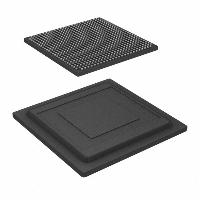
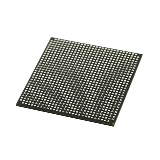
Arria V GX Field Programmable Gate Array (FPGA) IC 336 13284352 190000 672-BBGA, FCBGA |
|---|---|
| Quantity | 467 Available (as of June 18, 2026) |

| Product Category | Field Programmable Gate Array (FPGA) |
|---|---|
| Manufacturer | Intel |
| Manufacturing Status | Active |
| Manufacturer Standard Lead Time | 12 Weeks |
| Datasheet |
Specifications & Environmental
| Device Package | 672-FBGA (27x27) | Grade | Commercial | Operating Temperature | 0°C – 85°C | ||
|---|---|---|---|---|---|---|---|
| Package / Case | 672-BBGA, FCBGA | Number of I/O | 336 | Voltage | 1.07 V - 1.13 V | ||
| Mounting Method | Surface Mount | RoHS Compliance | RoHS Compliant | REACH Compliance | REACH Unaffected | ||
| Moisture Sensitivity Level | 3 (168 Hours) | Number of LABs/CLBs | 8962 | Number of Logic Elements/Cells | 190000 | ||
| Number of Gates | N/A | ECCN | PENDING ECCN | HTS Code | 0000.00.0000 | ||
| Qualification | N/A | Total RAM Bits | 13284352 |
Overview of 5AGXBA5D4F27C5G – Arria V GX FPGA, 190,000 logic elements, 672‑FBGA
The 5AGXBA5D4F27C5G is an Intel Arria V GX Field Programmable Gate Array (FPGA) supplied in a 672‑FBGA (27×27) surface‑mount package. It provides a large programmable fabric with 190,000 logic elements, 13,284,352 bits of on‑chip RAM, and 336 user I/O pins, making it suitable for system designs that require substantial logic capacity, significant embedded memory, and high I/O density.
Key Features
- Core Logic — 190,000 logic elements delivering large programmable capacity for complex logic implementation.
- Logic Blocks — 8,962 logic blocks to structure logic resources across the device.
- On‑Chip Memory — 13,284,352 total RAM bits for buffering, FIFOs, and local storage without external memory.
- I/O Density — 336 general‑purpose I/O pins to support extensive peripheral and interface connectivity.
- Power Supply — Core voltage specified between 1.07 V and 1.13 V to align with target power‑rail design.
- Package & Mounting — 672‑BBGA / FCBGA (672‑FBGA, 27×27) package in a surface‑mount format for board‑level integration.
- Operating Range — Commercial grade device rated for 0 °C to 85 °C ambient operation.
- Environmental Compliance — RoHS compliant to support regulatory and manufacturing requirements.
Typical Applications
- Programmable logic systems — Implement custom logic functions and data path processing using the device’s 190,000 logic elements.
- High‑I/O interface designs — Leverage 336 I/O pins to connect multiple peripherals, boards, or external interfaces.
- On‑chip memory‑centric designs — Use 13,284,352 bits of embedded RAM for buffering, packet storage, and local data handling without immediate external memory needs.
Unique Advantages
- Large programmable capacity: 190,000 logic elements enable implementation of complex algorithms and multi‑function systems on a single device.
- Substantial embedded RAM: Over 13 million bits of on‑chip RAM reduce reliance on external memory and simplify board design.
- High I/O count: 336 I/O pins provide flexibility for dense connectivity and multiple parallel interfaces.
- Surface‑mount 672‑FBGA package: Compact 27×27 FBGA package supports high‑density PCB layouts and standard SMT assembly processes.
- Commercial grade and RoHS compliant: Suitable for mainstream commercial deployments with regulatory environmental compliance.
- Defined core power window: Core supply specification of 1.07 V–1.13 V assists in precise power‑rail planning.
Why Choose 5AGXBA5D4F27C5G?
The 5AGXBA5D4F27C5G Arria V GX FPGA combines a large logic fabric, significant on‑chip RAM, and extensive I/O in a compact 672‑FBGA package. Its commercial operating range and RoHS compliance make it a practical choice for production designs that need high logic capacity and memory resources while maintaining a predictable power and thermal envelope.
Engineers and procurement teams looking to consolidate multiple functions into a single programmable device will find this part suitable for designs that demand dense logic, local memory, and broad connectivity, backed by Intel’s Arria V device specifications and documentation.
Request a quote or submit a pricing request to evaluate 5AGXBA5D4F27C5G for your next design.


Date Founded: 1968
Headquarters: Santa Clara, California, USA
Employees: 130,000+
Revenue: $54.23 Billion
Certifications and Memberships: ISO9001:2015, ISO14001:2015, ISO17025:2017, ISO27001:2022, ISO45001:2018, ISO50001:2018


