
5AGXBB5D4F35C5N
| Part Description |
Arria V GX Field Programmable Gate Array (FPGA) IC 544 23625728 420000 1152-BBGA, FCBGA Exposed Pad |
|---|---|
| Quantity | 137 Available (as of June 15, 2026) |

| Product Category | Field Programmable Gate Array (FPGA) |
|---|---|
| Manufacturer | Intel |
| Manufacturing Status | Obsolete |
| Manufacturer Standard Lead Time | Contact Us |
| Datasheet |
Specifications & Environmental
| Device Package | 1152-FBGA (35x35) | Grade | Commercial | Operating Temperature | 0°C – 85°C | ||
|---|---|---|---|---|---|---|---|
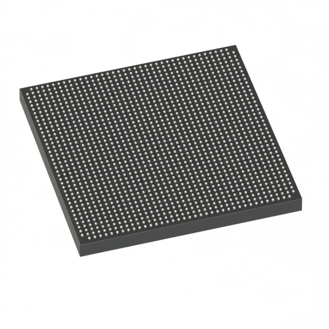
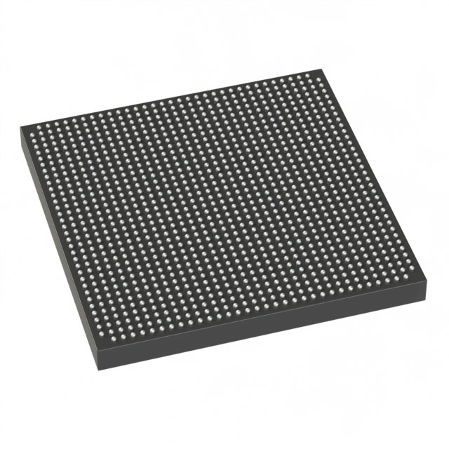
| Package / Case | 1152-BBGA, FCBGA Exposed Pad | Number of I/O | 544 | Voltage | 1.07 V - 1.13 V | ||
| Mounting Method | Surface Mount | RoHS Compliance | RoHS Compliant | REACH Compliance | REACH Unknown | ||
| Moisture Sensitivity Level | 3 (168 Hours) | Number of LABs/CLBs | 19811 | Number of Logic Elements/Cells | 420000 | ||
| Number of Gates | N/A | ECCN | 3A001A2C | HTS Code | 8542.39.0001 | ||
| Qualification | N/A | Total RAM Bits | 23625728 |
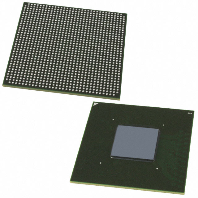
Overview of 5AGXBB5D4F35C5N – Arria V GX FPGA, 420,000 logic elements, 544 I/Os, 1152-BBGA
The 5AGXBB5D4F35C5N is an Arria V GX Field Programmable Gate Array (FPGA) in a 1152-BBGA exposed-pad package designed for commercial embedded applications. It integrates high logic density, substantial on-chip memory, and a large I/O count to support complex logic implementations in commercial designs.
A comprehensive device datasheet is available that documents electrical characteristics, switching characteristics, configuration specifications, and I/O timing for Arria V devices.
Key Features
- Logic Capacity Approximately 420,000 logic elements and 19,811 CLBs provide a high-density fabric for implementing complex logic and state machines.
- Embedded Memory Approximately 23.6 Mbits of on-chip RAM for buffering, packet processing, and local storage within the FPGA fabric.
- I/O Resources 544 general-purpose I/O pins enable broad interfacing capability for parallel buses, control signals, and external peripherals.
- Power and Operating Range Core voltage supply range specified at 1.07 V to 1.13 V; commercial operating temperature range of 0 °C to 85 °C.
- Package and Mounting 1152-BBGA FCBGA with exposed pad (supplier package: 1152-FBGA, 35×35); surface-mount package suitable for standard PCB assembly.
- Compliance RoHS compliant.
- Documentation Datasheet content covers electrical characteristics, switching characteristics, configuration specifications (including POR and various configuration modes), and I/O timing details.
Typical Applications
- Commercial embedded systems Implement complex control, protocol bridging, or custom acceleration in commercial products that require a high logic count and extensive I/O.
- High-channel I/O designs Systems needing dozens to hundreds of external signals can use the 544 I/Os for parallel interfaces, aggregation, or multi-channel control.
- On-chip memory dependent functions Applications that require local buffering, packet storage, or lookup tables can leverage approximately 23.6 Mbits of embedded memory.
Unique Advantages
- High logic density: The combination of ~420,000 logic elements and 19,811 CLBs supports sophisticated logic architectures without immediate need for external logic chips.
- Substantial embedded memory: Approximately 23.6 Mbits of on-chip RAM reduces dependence on external memory for many buffering and storage tasks, simplifying board design.
- Large I/O complement: 544 I/Os gives designers flexibility to connect multiple peripherals, busses, and I/O domains directly to the FPGA.
- Commercial-grade readiness: Specified for 0 °C to 85 °C operation and RoHS compliance for deployment in commercial environments.
- Exposed-pad BGA package: 1152-BBGA with exposed pad and surface-mount mounting supports thermal management and standard PCB assembly flow.
Why Choose 5AGXBB5D4F35C5N?
The 5AGXBB5D4F35C5N Arria V GX FPGA combines a high logic element count, significant on-chip memory, and extensive I/O resources in a commercially rated, RoHS-compliant BGA package. It is well suited to designers seeking to consolidate logic, memory, and I/O into a single programmable device for commercial embedded applications.
Designed for projects that require scalable logic capacity and flexible interfacing, this device provides detailed documentation on electrical, switching, configuration, and I/O timing to support robust implementation and verification in commercial product designs.
Request a quote or submit a purchase inquiry to receive pricing and availability information for 5AGXBB5D4F35C5N. Include your required quantities and delivery expectations to expedite a response.


Date Founded: 1968
Headquarters: Santa Clara, California, USA
Employees: 130,000+
Revenue: $54.23 Billion
Certifications and Memberships: ISO9001:2015, ISO14001:2015, ISO17025:2017, ISO27001:2022, ISO45001:2018, ISO50001:2018


