
5AGXFB3H4F35C5N
| Part Description |
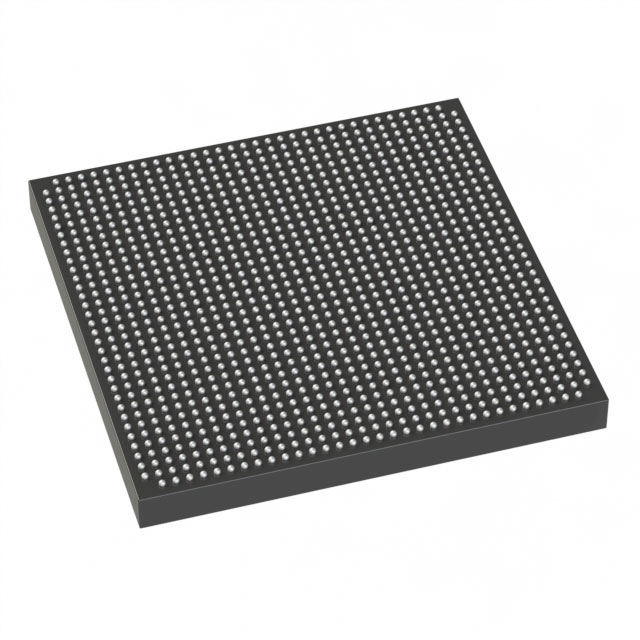
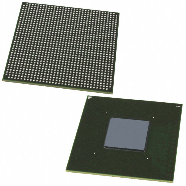
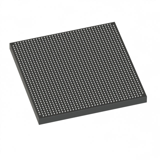
Arria V GX Field Programmable Gate Array (FPGA) IC 544 19822592 362000 1152-BBGA, FCBGA Exposed Pad |
|---|---|
| Quantity | 781 Available (as of June 15, 2026) |

| Product Category | Field Programmable Gate Array (FPGA) |
|---|---|
| Manufacturer | Intel |
| Manufacturing Status | Obsolete |
| Manufacturer Standard Lead Time | Contact Us |
| Datasheet |
Specifications & Environmental
| Device Package | 1152-FBGA (35x35) | Grade | Commercial | Operating Temperature | 0°C – 85°C | ||
|---|---|---|---|---|---|---|---|
| Package / Case | 1152-BBGA, FCBGA Exposed Pad | Number of I/O | 544 | Voltage | 1.07 V - 1.13 V | ||
| Mounting Method | Surface Mount | RoHS Compliance | RoHS Compliant | REACH Compliance | REACH Unknown | ||
| Moisture Sensitivity Level | 3 (168 Hours) | Number of LABs/CLBs | 17110 | Number of Logic Elements/Cells | 362000 | ||
| Number of Gates | N/A | ECCN | 3A001A2C | HTS Code | 8542.39.0001 | ||
| Qualification | N/A | Total RAM Bits | 19822592 |
Overview of 5AGXFB3H4F35C5N – Arria V GX FPGA, 544 I/Os, ~19.8 Mbits RAM, 362,000 logic elements, 1152‑BBGA
The 5AGXFB3H4F35C5N is an Intel Arria V GX Field Programmable Gate Array (FPGA) supplied in a 1152‑BBGA exposed‑pad package. It delivers a large logic capacity and embedded RAM in a surface‑mount FCBGA footprint, making it suitable for designs that require extensive on‑chip logic, significant embedded memory, and a high‑count I/O interface.
Designed for commercial applications, this device operates over a 0 °C to 85 °C temperature range and requires a core supply between 1.07 V and 1.13 V. The part is RoHS compliant and packaged as a 1152‑FBGA (35×35) device for board‑level integration.
Key Features
- Large Logic Capacity — Approximately 362,000 logic elements to implement complex digital systems and large custom logic functions.
- Embedded Memory — Approximately 19.8 Mbits of on‑chip RAM for data buffering, on‑chip storage, and state machines.
- High I/O Count — 544 I/O pins to support dense peripheral interfacing and multi‑lane connectivity on a single device.
- Package and Mounting — 1152‑BBGA, FCBGA exposed pad (1152‑FBGA, 35×35) in a surface‑mount configuration for compact board footprints and thermal connection via the exposed pad.
- Power and Operating Range — Core voltage supply specified from 1.07 V to 1.13 V to match system power sequencing; commercial temperature grade with an operating range of 0 °C to 85 °C.
- Compliance — RoHS compliant for environmentally regulated assemblies.
Typical Applications
- System Integration and Prototyping — Use the device for complex FPGA‑based prototypes and system integration tasks that need substantial logic and embedded memory capacity.
- I/O‑Rich Interface Consolidation — Suitable for designs that consolidate multiple peripheral interfaces or require many parallel I/O connections.
- Embedded Data Processing — On‑chip RAM and large logic fabric support buffering and custom data‑path implementations within embedded systems.
- Control and Signal Management — Deploy where dense control logic and deterministic hardware implementation are required across many signals.
Unique Advantages
- High Integration Density: Large logic element count and substantial embedded RAM reduce the need for external logic and memory components.
- Extensive I/O Capacity: 544 I/Os enable consolidation of multiple interfaces and simplify board‑level routing for complex systems.
- Compact, Thermally Friendly Package: 1152‑BBGA with exposed pad supports compact layouts and provides a path for board‑level thermal management.
- Commercial Temperature Grade: Rated for 0 °C to 85 °C, suitable for a wide range of commercial electronic products.
- Standards‑conscious Manufacturing: RoHS compliance aligns the device with modern environmental and manufacturing requirements.
Why Choose 5AGXFB3H4F35C5N?
The 5AGXFB3H4F35C5N Arria V GX FPGA combines a large logic fabric, nearly 20 Mbits of embedded RAM, and a high‑count I/O complement in a compact 1152‑BBGA package, offering a balanced platform for commercial designs that require significant on‑chip resources and dense external interfacing. Its specified core voltage range and commercial temperature rating make it suitable for mainstream embedded and system‑level applications.
This part is well suited to engineers and procurement teams seeking a high‑capacity FPGA from Intel for integration into boards where logic density, embedded memory, and I/O count are primary selection criteria. The RoHS compliance and surface‑mount FCBGA packaging support modern assembly and environmental standards.
Request a quote or submit an inquiry for 5AGXFB3H4F35C5N to obtain pricing and availability information for your next design.


Date Founded: 1968
Headquarters: Santa Clara, California, USA
Employees: 130,000+
Revenue: $54.23 Billion
Certifications and Memberships: ISO9001:2015, ISO14001:2015, ISO17025:2017, ISO27001:2022, ISO45001:2018, ISO50001:2018


