
5AGXMA3D4F31C5N
| Part Description |
Arria V GX Field Programmable Gate Array (FPGA) IC 416 11746304 156000 896-BBGA, FCBGA |
|---|---|
| Quantity | 530 Available (as of June 15, 2026) |

| Product Category | Field Programmable Gate Array (FPGA) |
|---|---|
| Manufacturer | Intel |
| Manufacturing Status | Obsolete |
| Manufacturer Standard Lead Time | Contact Us |
| Datasheet |
Specifications & Environmental
| Device Package | 896-FBGA (31x31) | Grade | Commercial | Operating Temperature | 0°C – 85°C | ||
|---|---|---|---|---|---|---|---|
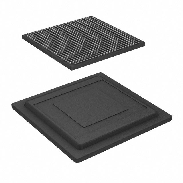
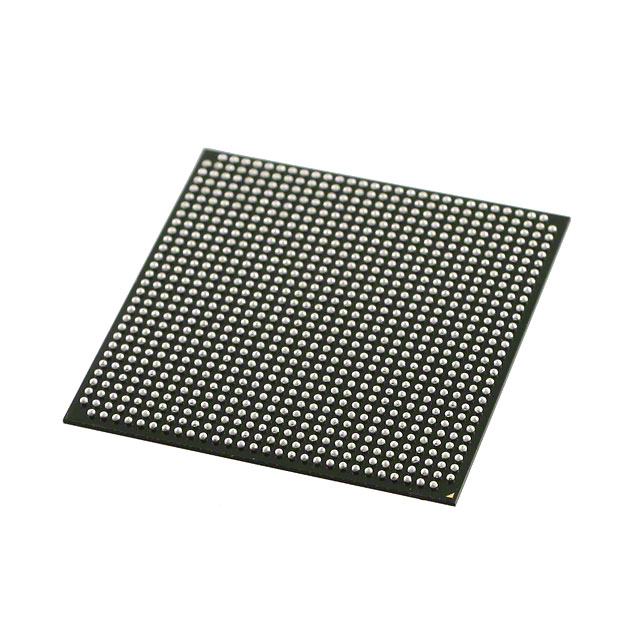
| Package / Case | 896-BBGA, FCBGA | Number of I/O | 416 | Voltage | 1.07 V - 1.13 V | ||
| Mounting Method | Surface Mount | RoHS Compliance | RoHS Compliant | REACH Compliance | REACH Unknown | ||
| Moisture Sensitivity Level | 3 (168 Hours) | Number of LABs/CLBs | 7362 | Number of Logic Elements/Cells | 156000 | ||
| Number of Gates | N/A | ECCN | 3A001A2C | HTS Code | 8542.39.0001 | ||
| Qualification | N/A | Total RAM Bits | 11746304 |
Overview of 5AGXMA3D4F31C5N – Arria V GX Field Programmable Gate Array, 156,000 Logic Elements, 416 I/Os
The 5AGXMA3D4F31C5N is an Arria V GX field programmable gate array (FPGA) in a commercial-grade, surface-mount FCBGA package. It integrates a large logic fabric and on-chip memory to support complex digital designs for commercial applications.
With 156,000 logic elements, approximately 11.7 Mbits of embedded memory, and 416 general-purpose I/O pins in an 896-ball BGA (31 × 31) footprint, this device is positioned for mid-to-high complexity designs that require significant logic and memory resources within a compact board footprint.
Key Features
- Core Logic 156,000 logic elements provide a substantial programmable fabric for implementing custom digital functions and parallel processing pipelines.
- Logic Blocks 7,362 logic blocks support hierarchical synthesis and resource partitioning for modular designs.
- Embedded Memory Approximately 11.7 Mbits of on-chip RAM to support buffers, FIFOs, and on-chip data storage without external memory for many functions.
- High-Density I/O 416 I/O pins permit extensive interfacing to peripherals, mezzanine modules, and board-level signals.
- Power and Voltage Core supply specified at 1.07 V to 1.13 V, enabling predictable supply requirements for power budgeting and voltage rail design.
- Package and Mounting 896-ball BGA FCBGA package (896-FBGA, 31 × 31) optimized for surface-mount assembly and compact PCB integration.
- Commercial Grade and Temperature Range Commercial-grade device with an operating temperature range of 0 °C to 85 °C for standard commercial environments.
- Compliance RoHS-compliant for regulatory and manufacturing compatibility.
Typical Applications
- Telecommunications & Networking Implements packet processing, protocol offload, and interface bridging using abundant logic resources and a high I/O count.
- Video and Image Processing Supports parallel data paths and buffering with large on-chip RAM and extensive logic for custom image pipelines.
- Industrial Control (Commercial Systems) Enables programmable control, signal aggregation, and protocol translation within commercial industrial equipment operating within the specified temperature range.
- Test & Measurement Facilitates custom digital front-ends, trigger logic, and data conditioning leveraging the device’s logic density and I/O capability.
Unique Advantages
- Substantial On-Chip Logic: 156,000 logic elements give designers the headroom to implement complex state machines, datapaths, and parallel processing without immediate partitioning to external devices.
- Integrated Memory Resources: Approximately 11.7 Mbits of embedded RAM reduce dependence on external memory for many buffering and lookup tasks, simplifying BOM and PCB routing.
- High I/O Count: 416 I/Os enable broad connectivity for multi-channel interfaces, sensor arrays, and mezzanine connections on dense system boards.
- Compact, Surface-Mount Package: 896-ball FCBGA (31 × 31) package supports high-density board layouts while maintaining a standard assembly flow for surface-mount technology.
- Predictable Power Envelope: A clearly defined core voltage range (1.07–1.13 V) assists in power-rail planning and board-level power design.
- Regulatory-Friendly: RoHS compliance aligns the device with modern manufacturing and environmental requirements.
Why Choose 5AGXMA3D4F31C5N?
The 5AGXMA3D4F31C5N combines a large programmable fabric, substantial embedded memory, and a high number of I/Os in a compact 896-ball FCBGA package, making it well suited for commercial designs that demand significant on-chip resources. Its defined core voltage range and commercial operating temperature range simplify integration into standard board designs and power architectures.
This device is appropriate for engineering teams building advanced commercial systems—where on-chip logic density, memory capacity, and connectivity must come together in a surface-mount FPGA solution backed by Arria V family documentation and electrical specifications.
Request a quote or submit an inquiry for part number 5AGXMA3D4F31C5N to receive pricing and availability information tailored to your project requirements.


Date Founded: 1968
Headquarters: Santa Clara, California, USA
Employees: 130,000+
Revenue: $54.23 Billion
Certifications and Memberships: ISO9001:2015, ISO14001:2015, ISO17025:2017, ISO27001:2022, ISO45001:2018, ISO50001:2018


