
5AGXMA3D4F31C4G
| Part Description |
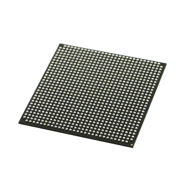
Arria V GX Field Programmable Gate Array (FPGA) IC 416 11746304 156000 896-BBGA, FCBGA |
|---|---|
| Quantity | 400 Available (as of October 7, 2026) |
| Product Category | Field Programmable Gate Array (FPGA) |
|---|---|
| Manufacturer | Intel |
| Manufacturing Status | Active |
| Manufacturer Standard Lead Time | 16 Weeks |
| Datasheet |
Specifications & Environmental
| Device Package | 896-FBGA (31x31) | Grade | Commercial | Operating Temperature | 0°C – 85°C | ||
|---|---|---|---|---|---|---|---|
| Package / Case | 896-BBGA, FCBGA | Number of I/O | 416 | Voltage | 1.07 V - 1.13 V | ||
| Mounting Method | Surface Mount | RoHS Compliance | RoHS Compliant | REACH Compliance | REACH Unaffected | ||
| Moisture Sensitivity Level | 3 (168 Hours) | Number of LABs/CLBs | 7362 | Number of Logic Elements/Cells | 156000 | ||
| Number of Gates | N/A | ECCN | 3A001A7A | HTS Code | 8542.39.0001 | ||
| Qualification | N/A | Total RAM Bits | 11746304 |
Overview of 5AGXMA3D4F31C4G – Arria V GX Field Programmable Gate Array (FPGA) IC
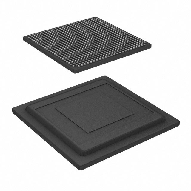
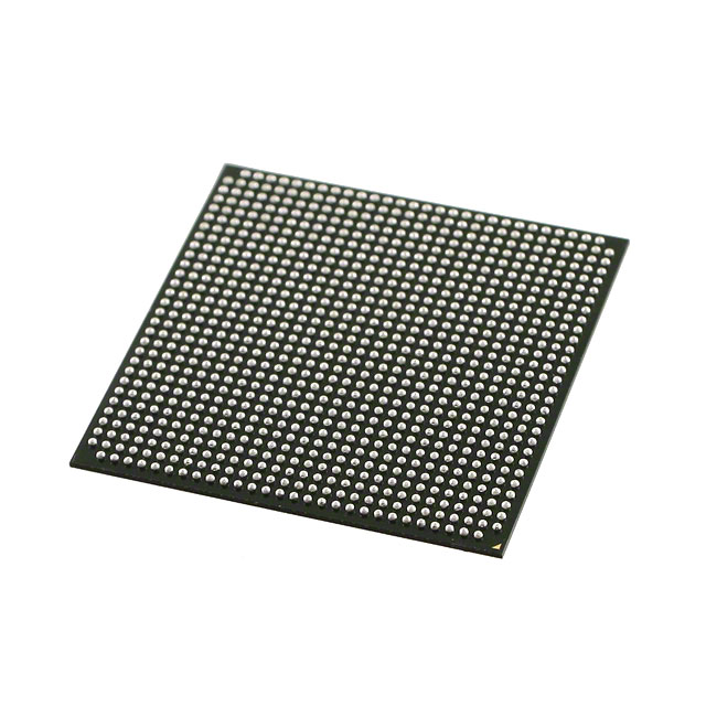
The 5AGXMA3D4F31C4G is an Intel Arria V GX FPGA in a 896-ball FCBGA package, offered as a commercial-grade programmable logic device. It provides 156,000 logic elements, approximately 11.75 Mbits of embedded RAM, and 416 user I/O pins, making it suitable for designs that require substantial on‑chip logic and memory in a single surface‑mount package.
Key technical references for the device family include electrical characteristics, switching characteristics, configuration specifications, and I/O timing information as documented in the Arria V device datasheet.
Key Features
- Logic Capacity — 156,000 logic elements to implement complex custom logic and datapaths.
- Embedded Memory — Total on‑chip RAM of 11,746,304 bits (approximately 11.75 Mbits) for buffering, FIFOs, and local storage.
- I/O Resources — 416 general‑purpose I/O pins to support wide parallel interfaces and flexible pinout assignments.
- Power Supply — Nominal core voltage range of 1.07 V to 1.13 V for core power planning and regulator selection.
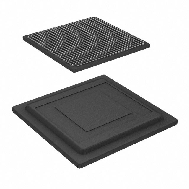
- Package — 896‑BBGA (FCBGA) package; supplier device package listed as 896‑FBGA (31×31) for board footprint and assembly planning.
- Mounting — Surface mount package suitable for standard PCB assembly processes.
- Operating Range & Grade — Commercial grade operation from 0 °C to 85 °C.
- Regulatory — RoHS compliant.
Typical Applications
- Custom programmable acceleration — Implement application‑specific datapaths and hardware accelerators using the device’s 156,000 logic elements and embedded memory.
- High‑I/O interface hubs — Support for dense parallel and mixed‑signal front‑ends with 416 user I/Os for aggregation and protocol bridging.
- Prototyping and validation — Commercial‑grade FPGA for board‑level prototyping where significant logic capacity and on‑chip RAM are required.
Unique Advantages
- Substantial on‑chip logic: 156,000 logic elements permit consolidation of functions that would otherwise require multiple discrete components.
- Significant embedded memory: Approximately 11.75 Mbits of RAM enables on‑chip buffering, block RAM usage, and reduced external memory dependence.
- High pin‑count connectivity: 416 I/O pins provide flexibility for complex interfacing and parallel channel support.
- Board‑level form factor: 896‑ball FCBGA (31×31) package balances density and routability for medium‑ to high‑complexity PCBs.
- Commercial temperature rating: 0 °C to 85 °C supports a wide range of customer electronics and embedded systems.
- Standards‑oriented supply planning: Defined core voltage range of 1.07 V to 1.13 V simplifies regulator selection and power budgeting.
Why Choose 5AGXMA3D4F31C4G?
This Arria V GX device combines large logic capacity, multi‑megabit on‑chip memory, and a high I/O count in a single commercial‑grade FCBGA package. It is well suited to customers who need a programmable, board‑level solution for consolidating complex logic, buffering large data streams, or implementing custom hardware functions without adding extensive external components.
Backed by detailed device documentation covering electrical, switching, configuration, and I/O timing characteristics, the 5AGXMA3D4F31C4G provides a verifiable platform for scalable designs where integration, predictable supply requirements, and RoHS compliance are required.
Request a quote or submit your procurement inquiry to evaluate the 5AGXMA3D4F31C4G for your next design. Technical documentation is available in the device datasheet to support hardware integration and system planning.





















Date Founded: 1968
Headquarters: Santa Clara, California, USA
Employees: 130,000+
Revenue: $54.23 Billion
Certifications and Memberships: ISO9001:2015, ISO14001:2015, ISO17025:2017, ISO27001:2022, ISO45001:2018, ISO50001:2018


