
5AGXMA3D4F31C4N
| Part Description |
Arria V GX Field Programmable Gate Array (FPGA) IC 416 11746304 156000 896-BBGA, FCBGA |
|---|---|
| Quantity | 229 Available (as of June 15, 2026) |

| Product Category | Field Programmable Gate Array (FPGA) |
|---|---|
| Manufacturer | Intel |
| Manufacturing Status | Obsolete |
| Manufacturer Standard Lead Time | Contact Us |
| Datasheet |
Specifications & Environmental
| Device Package | 896-FBGA (31x31) | Grade | Commercial | Operating Temperature | 0°C – 85°C | ||
|---|---|---|---|---|---|---|---|
| Package / Case | 896-BBGA, FCBGA | Number of I/O | 416 | Voltage | 1.07 V - 1.13 V | ||
| Mounting Method | Surface Mount | RoHS Compliance | RoHS Compliant | REACH Compliance | REACH Unknown | ||
| Moisture Sensitivity Level | 3 (168 Hours) | Number of LABs/CLBs | 7362 | Number of Logic Elements/Cells | 156000 | ||
| Number of Gates | N/A | ECCN | 3A001A2C | HTS Code | 8542.39.0001 | ||
| Qualification | N/A | Total RAM Bits | 11746304 |
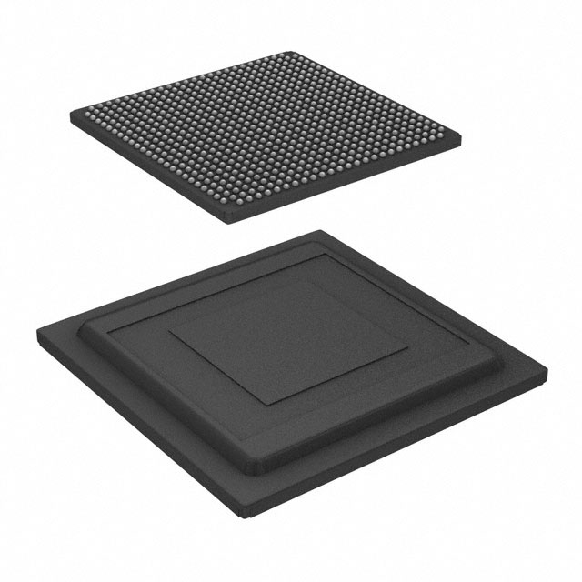
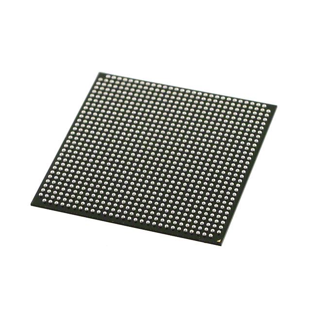
Overview of 5AGXMA3D4F31C4N – Arria V GX Field Programmable Gate Array (FPGA), 156000 logic elements
The 5AGXMA3D4F31C4N is an Arria V GX family Field Programmable Gate Array (FPGA) provided in a 896-BBGA FCBGA package. It delivers 156,000 logic elements, approximately 11.7 Mbits of embedded RAM, and a high I/O count for complex, programmable digital designs.
Targeted at commercial-grade applications, this device combines high-density programmable logic, substantial on-chip memory, and a broad I/O complement to support designs that require flexible, reconfigurable hardware with well-documented electrical and configuration specifications.
Key Features
- Logic Density 156,000 logic elements to implement complex custom logic, finite-state machines, and datapaths.
- Embedded Memory Approximately 11.7 Mbits of on-chip RAM suitable for buffering, FIFOs, and local storage.
- High I/O Count 416 general-purpose I/O pins to support wide parallel interfaces, peripherals, and complex board-level connectivity.
- Package & Mounting 896-BBGA (FCBGA) package in a 31 × 31 supplier device footprint; surface-mount mounting for compact board designs.
- Power Supply Core voltage supply range of 1.07 V to 1.13 V, enabling tight power budgeting and predictable core operation.
- Operating Grade & Temperature Commercial grade with an operating temperature range of 0 °C to 85 °C.
- Compliance RoHS-compliant for environmental and manufacturing considerations.
- Comprehensive Documentation Detailed datasheet coverage includes electrical characteristics, switching characteristics, configuration specifications, and I/O timing for design validation and integration.
Typical Applications
- High-density digital processing Implement custom datapaths, state machines, and parallel processing logic where 156,000 logic elements are required.
- Memory-buffered interfaces Use embedded RAM (≈11.7 Mbits) for buffering, packet storage, and latency-sensitive dataflows.
- Multi-interface boards Leverage 416 I/Os for complex peripheral connectivity, wide buses, and mixed-signal front-ends.
Unique Advantages
- Substantial logic capacity: Enables implementation of sizeable custom logic blocks and integration of multiple functions into a single device, reducing system complexity.
- On-chip memory for local storage: Approximately 11.7 Mbits of RAM minimizes external memory dependence for many buffering and temporary storage needs.
- High I/O density: 416 I/Os allow flexible board-level partitioning and support for parallel interfaces without additional I/O expanders.
- Compact FCBGA package: The 896-BBGA (31×31) footprint delivers high pin count in a compact surface-mount form factor for dense PCB layouts.
- Predictable power domain: Narrow core voltage range (1.07 V–1.13 V) simplifies core power supply design and regulation.
- Documented design guidance: Datasheet coverage of electrical, switching, and configuration specifications supports thorough design validation and reliable integration.
Why Choose 5AGXMA3D4F31C4N?
The 5AGXMA3D4F31C4N Arria V GX FPGA delivers a balanced combination of logic density, embedded memory, and I/O capacity in a compact FCBGA package for commercial-grade applications. Its documented electrical and configuration specifications make it suitable for projects that demand repeatable performance and clear integration requirements.
Engineers designing complex digital systems, memory-buffered interfaces, or multi-I/O boards will find this device appropriate where on-chip resources and a high pin count reduce external components and simplify board-level architecture.
Request a quote or submit a parts inquiry to obtain availability and pricing details for the 5AGXMA3D4F31C4N.


Date Founded: 1968
Headquarters: Santa Clara, California, USA
Employees: 130,000+
Revenue: $54.23 Billion
Certifications and Memberships: ISO9001:2015, ISO14001:2015, ISO17025:2017, ISO27001:2022, ISO45001:2018, ISO50001:2018


