
5AGXMA3D6F31C6G
| Part Description |
Arria V GX Field Programmable Gate Array (FPGA) IC 416 11746304 156000 896-BBGA, FCBGA |
|---|---|
| Quantity | 1,303 Available (as of June 14, 2026) |

| Product Category | Field Programmable Gate Array (FPGA) |
|---|---|
| Manufacturer | Intel |
| Manufacturing Status | Active |
| Manufacturer Standard Lead Time | 16 Weeks |
| Datasheet |
Specifications & Environmental
| Device Package | 896-FBGA (31x31) | Grade | Commercial | Operating Temperature | 0°C – 85°C | ||
|---|---|---|---|---|---|---|---|
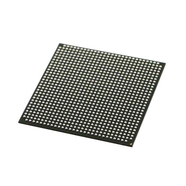
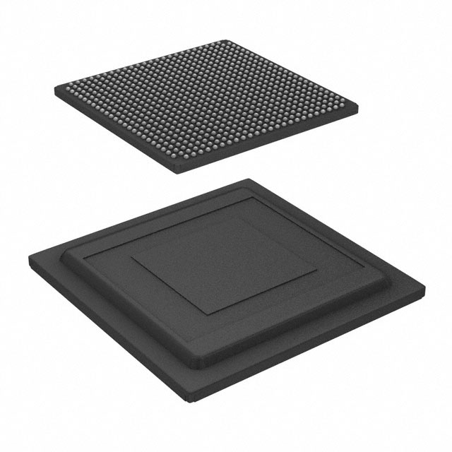
| Package / Case | 896-BBGA, FCBGA | Number of I/O | 416 | Voltage | 1.07 V - 1.13 V | ||
| Mounting Method | Surface Mount | RoHS Compliance | RoHS Compliant | REACH Compliance | REACH Unaffected | ||
| Moisture Sensitivity Level | 3 (168 Hours) | Number of LABs/CLBs | 7362 | Number of Logic Elements/Cells | 156000 | ||
| Number of Gates | N/A | ECCN | PENDING ECCN | HTS Code | 0000.00.0000 | ||
| Qualification | N/A | Total RAM Bits | 11746304 |
Overview of 5AGXMA3D6F31C6G – Arria V GX Field Programmable Gate Array (FPGA) IC
The 5AGXMA3D6F31C6G is an Arria V GX FPGA in a 896-ball BGA (FCBGA) package, designed for commercial embedded designs that require substantial programmable logic, on-chip memory, and large I/O counts. This device provides 156,000 logic elements and approximately 11.7 Mbits of embedded RAM, with 416 user I/O pins, making it suitable for complex system integration and high-density digital designs.
Packaged in a 896-FBGA (31×31) format for surface-mount assembly, the device operates from a core supply range of 1.07 V to 1.13 V and is rated for commercial temperature operation from 0 °C to 85 °C. The part is RoHS compliant.
Key Features
- High Logic Capacity — 156,000 logic elements provide substantial programmable fabric for complex logic and control implementations.
- Significant On-chip Memory — Approximately 11.7 Mbits of embedded RAM for data buffering, state storage, and on-chip packet or frame handling.
- Extensive I/O — 416 user I/O pins to support wide parallel interfaces, multi-channel connectivity, and flexible board-level routing.
- Package and Mounting — 896-BBGA FCBGA package (supplier device package: 896-FBGA, 31×31) optimized for surface-mount PCB assembly.
- Power and Supply — Core supply operating range of 1.07 V to 1.13 V for predictable power domain design.
- Commercial Grade Temperature — Rated for 0 °C to 85 °C operation to match a wide range of commercial applications.
- Regulatory — RoHS compliant for modern electronics manufacturing requirements.
Typical Applications
- High-density digital processing — Implement large custom datapaths and control logic where 156,000 logic elements and extensive embedded RAM accelerate on-chip processing.
- Multi-interface bridging — Use the 416 I/O pins to consolidate and translate between numerous parallel and serial interfaces on a single device.
- Embedded system control — Centralize glue logic, timing, and peripheral management in compact, surface-mount board designs using the 896-FBGA package.
- Prototyping and FPGA-based acceleration — Provide programmable hardware resources for design validation and proof-of-concept implementations in commercial product development.
Unique Advantages
- Substantial on-chip logic: 156,000 logic elements enable complex state machines, parallel processing, and integration of multiple functions into a single device.
- Ample embedded RAM: Approximately 11.7 Mbits of on-chip memory reduces reliance on external RAM for temporary data storage and buffering.
- High I/O density: 416 I/O pins allow broad system connectivity and flexible board-level partitioning without additional I/O expanders.
- Surface-mount, high-pin-count package: The 896-FBGA (31×31) package supports compact PCB layouts while providing many signals for complex designs.
- Commercial operation and compliance: Commercial temperature rating (0 °C to 85 °C) and RoHS compliance simplify integration into consumer and industrial electronics supply chains.
Why Choose 5AGXMA3D6F31C6G?
This Arria V GX FPGA balances high programmable logic density, on-chip memory, and extensive I/O in a single, surface-mount 896-FBGA package. Its electrical operating range and commercial temperature rating make it suitable for a wide range of commercial embedded systems that require significant logic resources and on-board memory without external component proliferation.
Designers seeking a scalable, high-density FPGA for integration-focused projects will appreciate the combination of 156,000 logic elements, approximately 11.7 Mbits of embedded RAM, and 416 I/O pins. The device’s package and supply characteristics support compact, manufacturable designs with RoHS compliance for modern production requirements.
Request a quote or submit a procurement inquiry to evaluate the 5AGXMA3D6F31C6G for your next design and receive pricing and availability details.


Date Founded: 1968
Headquarters: Santa Clara, California, USA
Employees: 130,000+
Revenue: $54.23 Billion
Certifications and Memberships: ISO9001:2015, ISO14001:2015, ISO17025:2017, ISO27001:2022, ISO45001:2018, ISO50001:2018


