
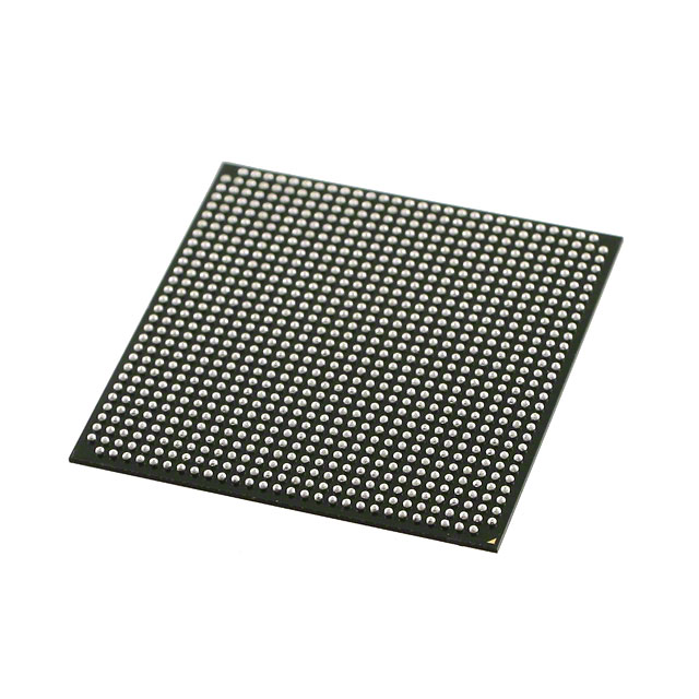
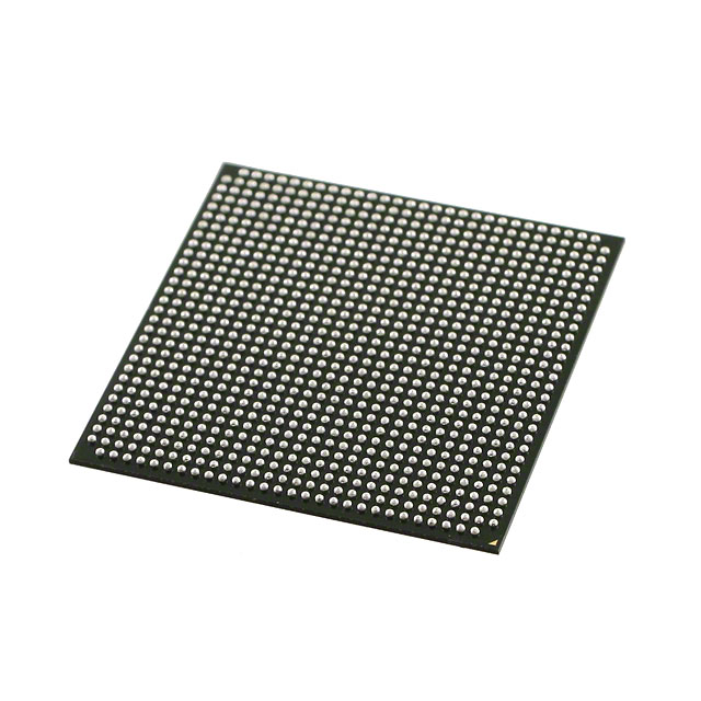
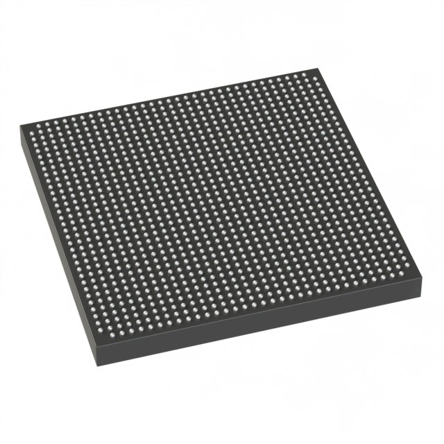
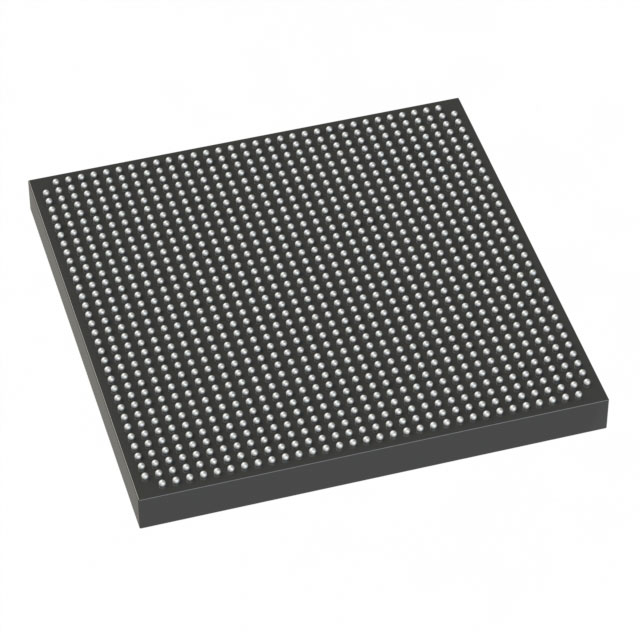
5AGXMA7G6F31C6G
| Part Description |
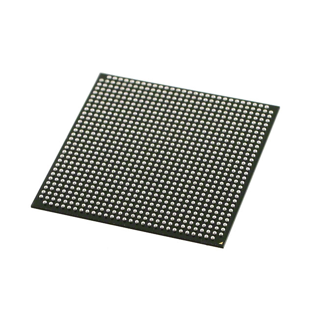
Arria V GX Field Programmable Gate Array (FPGA) IC 384 15470592 242000 896-BBGA, FCBGA |
|---|---|
| Quantity | 942 Available (as of October 8, 2026) |
| Product Category | Field Programmable Gate Array (FPGA) |
|---|---|
| Manufacturer | Intel |
| Manufacturing Status | Active |
| Manufacturer Standard Lead Time | 12 Weeks |
| Datasheet |
Specifications & Environmental
| Device Package | 896-FBGA (31x31) | Grade | Commercial | Operating Temperature | 0°C – 85°C | ||
|---|---|---|---|---|---|---|---|
| Package / Case | 896-BBGA, FCBGA | Number of I/O | 384 | Voltage | 1.07 V - 1.13 V | ||
| Mounting Method | Surface Mount | RoHS Compliance | RoHS Compliant | REACH Compliance | REACH Unaffected | ||
| Moisture Sensitivity Level | 3 (168 Hours) | Number of LABs/CLBs | 11460 | Number of Logic Elements/Cells | 242000 | ||
| Number of Gates | N/A | ECCN | PENDING ECCN | HTS Code | 0000.00.0000 | ||
| Qualification | N/A | Total RAM Bits | 15470592 |
Overview of 5AGXMA7G6F31C6G – Arria V GX Field Programmable Gate Array (FPGA) IC, 384 I/O, 242,000 Logic Elements
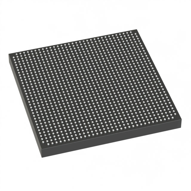
The 5AGXMA7G6F31C6G is an Arria V GX Field Programmable Gate Array (FPGA) IC manufactured by Intel. This commercial‑grade device delivers a large programmable fabric with substantial on‑chip memory and a high count of I/O pins, packaged in an 896‑FBGA (31×31) surface‑mount package.
Designed for systems that require dense programmable logic, abundant embedded RAM, and extensive I/O, the device operates from a core voltage range of 1.07 V to 1.13 V and across a commercial temperature range of 0 °C to 85 °C. The part is RoHS compliant and supplied in a 896‑BBGA FCBGA package.
Key Features
- Large logic capacity — 242,000 logic elements provide substantial programmable logic for complex designs and integration of custom functions.
- On‑chip memory — Approximately 15.47 Mbits of embedded memory to support buffering, lookup tables, and state storage within the FPGA fabric.
- High I/O count — 384 user I/O pins to accommodate multiple interfaces, peripherals, and high‑pin‑count designs.
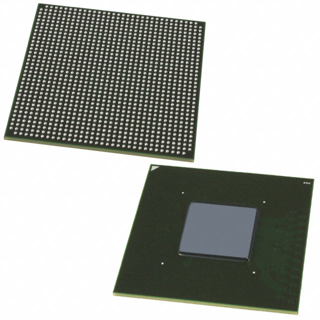
- Package and mounting — 896‑FBGA (31×31) package case in an 896‑BBGA, FCBGA format; surface‑mount device suitable for board‑level assembly.
- Power and operating conditions — Core supply range of 1.07 V to 1.13 V; commercial operating temperature range of 0 °C to 85 °C.
- Compliance — RoHS compliant, aligning with common environmental requirements for electronic assemblies.
Typical Applications
- Programmable system integration — Use the large logic capacity and abundant I/O to implement custom glue logic, protocol bridging, and mixed‑signal control functions within a single device.
- Memory‑intensive processing — Approximately 15.47 Mbits of embedded RAM supports buffering, lookup operations, and on‑chip data storage for streaming or packetized data flows.
- I/O‑heavy designs — The 384 I/O pins allow designers to connect multiple peripherals and external interfaces without sacrificing board real estate.
Unique Advantages
- High logic density: 242,000 logic elements enable complex custom logic implementations and feature consolidation.
- Substantial embedded memory: Approximately 15.47 Mbits of on‑chip RAM reduces dependence on external memory for many buffering and processing tasks.
- Extensive I/O capability: 384 I/O pins support multi‑interface designs and simplify routing of external signals.
- Commercial readiness: Rated for 0 °C to 85 °C operation and provided in a surface‑mount 896‑FBGA (31×31) package for production PCB assembly.
- Regulatory alignment: RoHS compliance supports environmental requirements for modern electronic products.
Why Choose 5AGXMA7G6F31C6G?
The 5AGXMA7G6F31C6G positions itself as a high‑capacity, commercial‑grade Arria V GX FPGA suitable for designs that require many logic resources, significant embedded RAM, and a large number of I/O connections. Its 896‑FBGA (31×31) package and surface‑mount mounting make it compatible with standard production assembly flows, while the defined core voltage window and operating temperature range provide predictable electrical and thermal operating points.
Backed by Intel's Arria V device documentation, this FPGA is appropriate for engineers and procurement teams looking to consolidate functions into a single programmable device while maintaining traceable electrical and environmental specifications.
Request a quote or submit your specifications to evaluate 5AGXMA7G6F31C6G for your next design or production run.





















Date Founded: 1968
Headquarters: Santa Clara, California, USA
Employees: 130,000+
Revenue: $54.23 Billion
Certifications and Memberships: ISO9001:2015, ISO14001:2015, ISO17025:2017, ISO27001:2022, ISO45001:2018, ISO50001:2018


