
5AGZME5K2F40C3G
| Part Description |
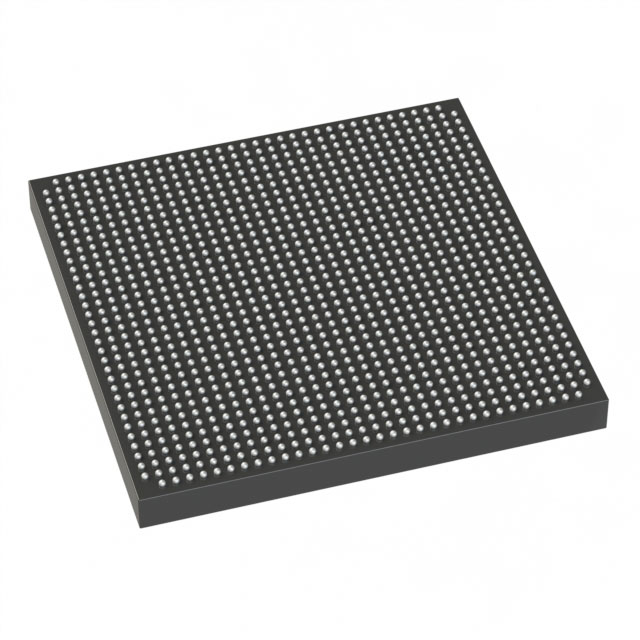
Arria V GZ Field Programmable Gate Array (FPGA) IC 674 34322432 400000 1517-BBGA, FCBGA |
|---|---|
| Quantity | 334 Available (as of June 15, 2026) |

| Product Category | Field Programmable Gate Array (FPGA) |
|---|---|
| Manufacturer | Intel |
| Manufacturing Status | Active |
| Manufacturer Standard Lead Time | 12 Weeks |
| Datasheet |
Specifications & Environmental
| Device Package | 1517-FBGA (40x40) | Grade | Commercial | Operating Temperature | 0°C – 85°C | ||
|---|---|---|---|---|---|---|---|
| Package / Case | 1517-BBGA, FCBGA | Number of I/O | 674 | Voltage | 820 mV - 880 mV | ||
| Mounting Method | Surface Mount | RoHS Compliance | RoHS Compliant | REACH Compliance | REACH Unaffected | ||
| Moisture Sensitivity Level | 3 (168 Hours) | Number of LABs/CLBs | 18870 | Number of Logic Elements/Cells | 400000 | ||
| Number of Gates | N/A | ECCN | N/A | HTS Code | N/A | ||
| Qualification | N/A | Total RAM Bits | 34322432 |
Overview of 5AGZME5K2F40C3G – Arria V GZ Field Programmable Gate Array (FPGA)
The 5AGZME5K2F40C3G is an Intel Arria V GZ Field Programmable Gate Array (FPGA) supplied in a 1517-BBGA (FCBGA) package. It provides high logic density, substantial on-chip memory, and a large I/O count for complex digital designs.
With approximately 400,000 logic elements, roughly 34.3 Mbits of embedded memory, and up to 674 I/O, this commercial-grade device is suited to applications that require dense programmable logic, significant local RAM, and extensive external interfacing while operating within a 0 °C to 85 °C range.
Key Features
- Core Logic Approximately 400,000 logic elements for high-density programmable logic implementation.
- Embedded Memory Approximately 34.3 Mbits of on-chip RAM to support buffering, lookup tables, and local data storage.
- I/O Capacity Up to 674 general-purpose I/O pins to support large multi-device interfaces and board-level connectivity.
- Power Requirements Core supply operating range of 820 mV to 880 mV, enabling defined power planning for system designs.
- Package & Mounting 1517-BBGA FCBGA package (supplier device package: 1517-FBGA, 40×40) with surface-mount mounting for compact, high-density PCB layouts.
- Commercial Grade & Temperature Range Commercial-grade device rated for operation from 0 °C to 85 °C.
- Regulatory RoHS compliant.
Typical Applications
- High-density digital processing Implement complex logic and parallel processing functions using the device’s approximately 400,000 logic elements and embedded RAM.
- Multi-interface systems Support boards and modules that require extensive external connectivity with up to 674 I/O pins for sensors, peripherals, and bridges.
- Prototyping and system integration Use as a programmable platform when on-chip memory and flexible I/O mapping are needed during development and integration.
- Embedded control and data buffering Leverage ~34.3 Mbits of on-chip RAM for local buffering, FIFOs, and temporary data storage in control systems.
Unique Advantages
- High logic density: Approximately 400,000 logic elements enable consolidation of multi-chip functions into a single FPGA, reducing board-level complexity.
- Substantial on-chip RAM: About 34.3 Mbits of embedded memory supports data-intensive operations without immediate external memory dependence.
- Extensive I/O capability: 674 I/O pins provide flexibility for complex interfacing and mixed-signal front ends.
- Compact system footprint: 1517-FBGA (40×40) package and surface-mount mounting support dense PCB designs and compact module layouts.
- Defined operating envelope: Commercial-grade rating and 0 °C to 85 °C operating range simplify thermal and reliability planning for commercial products.
- RoHS compliant: Meets common environmental compliance expectations for assembly and manufacturing.
Why Choose 5AGZME5K2F40C3G?
The 5AGZME5K2F40C3G Arria V GZ FPGA is positioned for designs that need a combination of high logic capacity, significant embedded RAM, and a large number of I/O in a compact FCBGA package. Its commercial-grade rating and defined supply voltage range make it straightforward to integrate into commercial electronic products and development platforms.
This part is suitable for engineers and OEMs building systems that require dense programmable logic resources, substantial on-chip memory, and broad external connectivity while maintaining a compact PCB footprint and predictable operating conditions.
If you would like pricing, availability, or to request a quote for 5AGZME5K2F40C3G, submit an inquiry or request a quote through your preferred procurement channel.


Date Founded: 1968
Headquarters: Santa Clara, California, USA
Employees: 130,000+
Revenue: $54.23 Billion
Certifications and Memberships: ISO9001:2015, ISO14001:2015, ISO17025:2017, ISO27001:2022, ISO45001:2018, ISO50001:2018


