
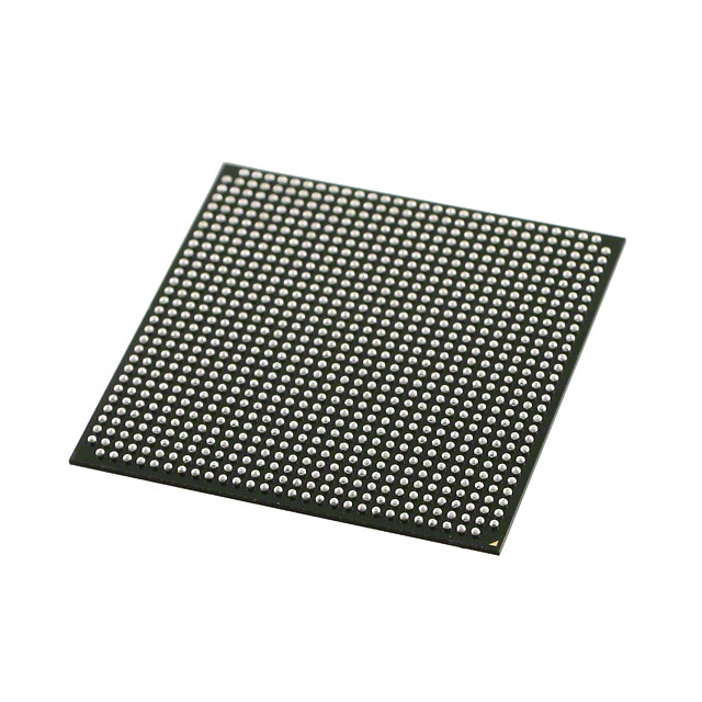
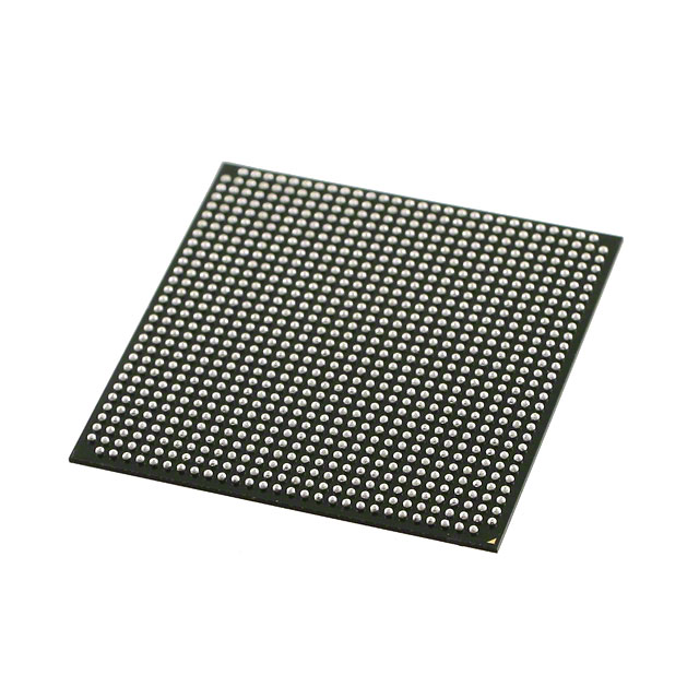
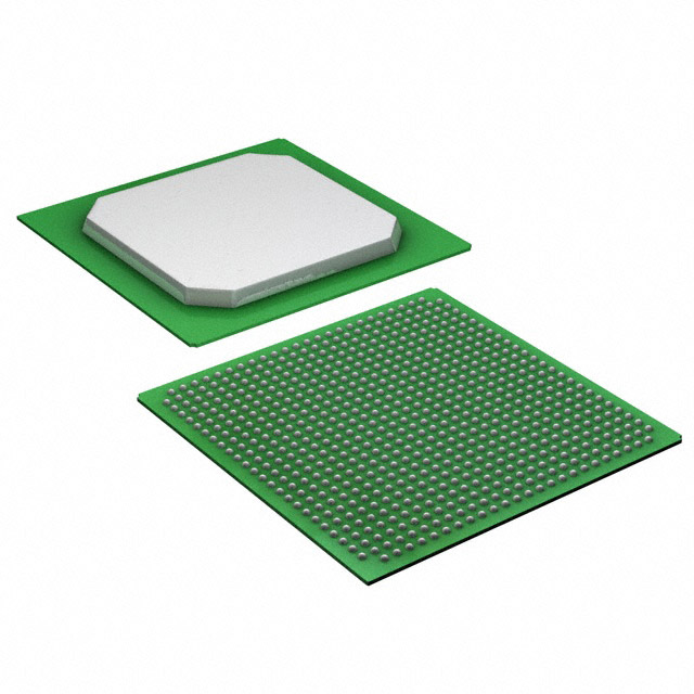
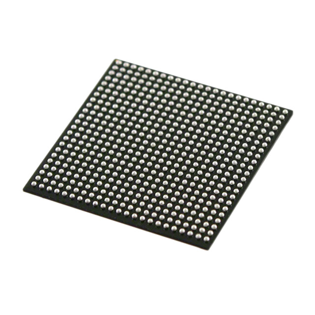
5CEBA9F31C7N
| Part Description |
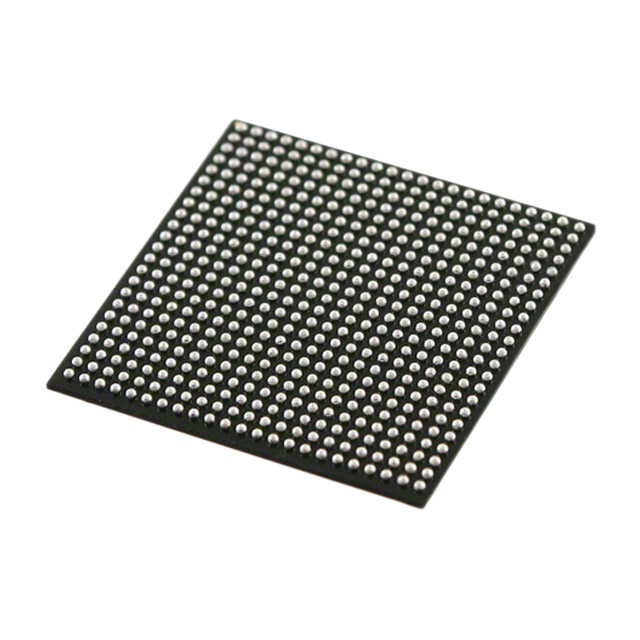
Cyclone® V E Field Programmable Gate Array (FPGA) IC 480 14251008 301000 896-BGA |
|---|---|
| Quantity | 681 Available (as of October 8, 2026) |
| Product Category | Field Programmable Gate Array (FPGA) |
|---|---|
| Manufacturer | Intel |
| Manufacturing Status | Active |
| Manufacturer Standard Lead Time | 16 Weeks |
| Datasheet |
Specifications & Environmental
| Device Package | 896-FBGA (31x31) | Grade | Commercial | Operating Temperature | 0°C – 85°C | ||
|---|---|---|---|---|---|---|---|
| Package / Case | 896-BGA | Number of I/O | 480 | Voltage | 1.07 V - 1.13 V | ||
| Mounting Method | Surface Mount | RoHS Compliance | RoHS Compliant | REACH Compliance | REACH Unaffected | ||
| Moisture Sensitivity Level | 3 (168 Hours) | Number of LABs/CLBs | 113560 | Number of Logic Elements/Cells | 301000 | ||
| Number of Gates | N/A | ECCN | 3A991D | HTS Code | 8542.39.0001 | ||
| Qualification | N/A | Total RAM Bits | 14251008 |
Overview of 5CEBA9F31C7N – Cyclone® V E FPGA, 301,000 logic elements, 480 I/O, 896-BGA
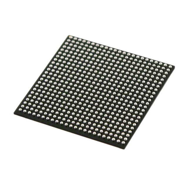
The 5CEBA9F31C7N is an Intel Cyclone® V E field-programmable gate array (FPGA) supplied in a 896-BGA (896-FBGA, 31 × 31) surface-mount package. Built on TSMC's 28 nm low-power process and featuring integrated transceivers and hard memory controllers (Cyclone V family capabilities), this device targets cost- and power-sensitive applications that require substantial programmable logic and on-chip memory.
With 301,000 logic elements, approximately 14.25 Mbits of embedded memory, and up to 480 I/O, the device supports dense, high-functionality designs across industrial, wireless and wireline, and military markets where commercial-grade operation (0 °C to 85 °C) and RoHS compliance are required.
Key Features
- Process and Core — TSMC 28 nm low-power technology with a nominal core supply range of 1.07 V to 1.13 V (1.1 V core), enabling reduced static and dynamic power for high-density designs.
- Logic Resources — 301,000 logic elements to implement large, complex digital functions and custom hardware acceleration.
- Embedded Memory — Approximately 14.25 Mbits of on-chip RAM with Cyclone V family memory architectures (including M10K blocks and ECC options referenced in the device family documentation).
- DSP and ALM — Family-level features include enhanced 8-input adaptive logic modules and variable-precision DSP blocks for arithmetic and signal processing workloads.
- I/O and Packaging — Up to 480 general-purpose I/O pins in a 896-FBGA (31 × 31) surface-mount package for high-density board-level interfacing.
- Integrated High-Speed Interfaces — Cyclone V family documentation references integrated transceivers and hard memory controllers to support high-bandwidth external interfaces.
- Operating Range and Compliance — Commercial-grade operation from 0 °C to 85 °C and RoHS-compliant supply status.
Typical Applications
- Industrial equipment — Use in control systems and instrumentation that benefit from high logic counts, embedded memory, and low-power operation.
- Wireless and wireline systems — Deploy where integrated transceivers and high-bandwidth memory interfaces are advantageous for data transport and protocol processing.
- Defense and military systems — Applicable to selected military designs that leverage substantial programmable logic and on-chip memory (note: device grade is Commercial; verify system-level qualification requirements).
Unique Advantages
- High-density programmable fabric — 301,000 logic elements provide capacity for complex control, signal-processing, and protocol-implementation tasks without immediate need for external ASICs.
- Substantial on-chip memory — Approximately 14.25 Mbits of embedded RAM reduces dependence on external memory for many application architectures, simplifying board design.
- Robust I/O in a compact package — 480 I/O in a 896-FBGA (31 × 31) offers a balance of connectivity and board-space efficiency for high-pin-count designs.
- Low-voltage core operation — Narrow core supply range (1.07 V–1.13 V) supports low-power system designs when combined with the 28 nm low-power process.
- Family-level integration options — Cyclone V family features such as integrated transceivers, hard memory controllers, adaptive logic modules, and variable-precision DSP blocks enable system consolidation and reduced BOM.
- Regulatory and manufacturing readiness — Surface-mount 896-FBGA package and RoHS compliance facilitate volume manufacturing and regulatory alignment.
Why Choose 5CEBA9F31C7N?
The 5CEBA9F31C7N delivers a high-capacity, low-power FPGA solution in a compact 896-BGA package. Its combination of 301,000 logic elements, approximately 14.25 Mbits of embedded memory, and up to 480 I/O makes it well-suited for commercial applications that require significant programmable resources and on-chip storage while maintaining power efficiency and a small board footprint.
This device is appropriate for development teams and procurement groups building medium- to high-complexity digital systems in industrial, wireless/wireline, and select military applications who need a commercially graded, RoHS-compliant FPGA with strong family-level integration features.
Request a quote or submit a procurement inquiry to receive pricing and availability for 5CEBA9F31C7N.





















Date Founded: 1968
Headquarters: Santa Clara, California, USA
Employees: 130,000+
Revenue: $54.23 Billion
Certifications and Memberships: ISO9001:2015, ISO14001:2015, ISO17025:2017, ISO27001:2022, ISO45001:2018, ISO50001:2018


