
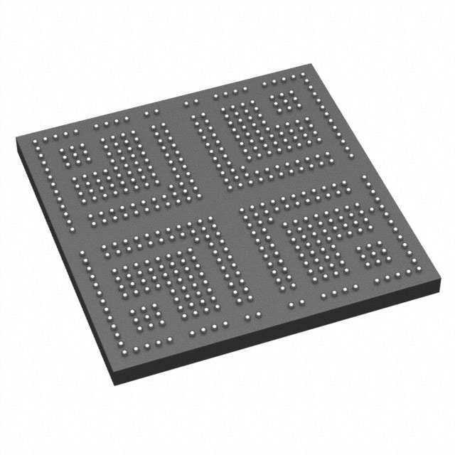
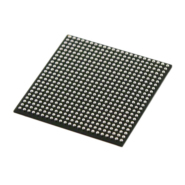
5CEFA7M15C8N
| Part Description |
Cyclone® V E Field Programmable Gate Array (FPGA) IC 240 7880704 149500 484-LFBGA |
|---|---|
| Quantity | 580 Available (as of June 15, 2026) |

| Product Category | Field Programmable Gate Array (FPGA) |
|---|---|
| Manufacturer | Intel |
| Manufacturing Status | Active |
| Manufacturer Standard Lead Time | 16 Weeks |
| Datasheet |
Specifications & Environmental
| Device Package | 484-MBGA (15x15) | Grade | Commercial | Operating Temperature | 0°C – 85°C | ||
|---|---|---|---|---|---|---|---|
| Package / Case | 484-LFBGA | Number of I/O | 240 | Voltage | 1.07 V - 1.13 V | ||
| Mounting Method | Surface Mount | RoHS Compliance | RoHS Compliant | REACH Compliance | REACH Unaffected | ||
| Moisture Sensitivity Level | 3 (168 Hours) | Number of LABs/CLBs | 56480 | Number of Logic Elements/Cells | 149500 | ||
| Number of Gates | N/A | ECCN | 3A001A2C | HTS Code | 8542.39.0001 | ||
| Qualification | N/A | Total RAM Bits | 7880704 |
Overview of 5CEFA7M15C8N – Cyclone V E Field Programmable Gate Array (FPGA), 240 I/O, 484-LFBGA
The 5CEFA7M15C8N is an Intel Cyclone V E series FPGA in a 484-LFBGA (484-MBGA, 15×15) surface-mount package. It delivers a high-capacity programmable fabric with substantial embedded memory and flexible I/O for cost-sensitive, high-bandwidth embedded and communications applications.
Engineered on TSMC 28 nm low-power process with a 1.1 V core nominal, this device targets industrial, wireless and wireline, and defense-focused systems that benefit from programmable logic, integrated hard IP, and efficient power characteristics.
Key Features
- Logic Capacity — Approximately 149,500 logic elements to support complex custom logic, protocol processing, and system integration.
- Embedded Memory — Approximately 7.88 Mbits of on-chip RAM for buffering, packet processing, and embedded data structures.
- I/O Density — 240 I/O pins to interface with a wide range of peripherals, memory, and high-speed links.
- Process and Core Voltage — Built on TSMC 28 nm low-power technology with a core supply operating range of 1.07 V to 1.13 V.
- High-speed Interfaces (family-level) — Cyclone V family includes integrated transceivers and hard memory controllers; family transceivers support multi-gigabit rates (documented at 3.125 Gbps and 6.144 Gbps in the device family overview).
- SoC and Hard IP (family-level) — Cyclone V family documentation describes variants with Hard Processor System (HPS) integration and hard IP blocks such as memory controllers and PCIe Gen1/Gen2.
- Package & Mounting — 484-LFBGA package (supplier package: 484-MBGA, 15×15) for surface-mount PCB assembly.
- Commercial Temperature Grade — Rated for 0 °C to 85 °C operation, suitable for commercial and many embedded applications.
- RoHS Compliant — Conforms to RoHS environmental requirements.
Typical Applications
- Wireless and Wireline Infrastructure — Use the device’s high logic capacity, embedded memory, and family-level transceiver capability for protocol processing, fronthaul/backhaul, and data-path acceleration.
- Embedded SoC Designs — Leverage Cyclone V family hard IP and HPS options for tightly integrated processor-plus-FPGA solutions in edge compute and control platforms.
- Industrial Systems — Integrate control, I/O aggregation, and deterministic logic functions using the device’s programmable fabric and 240 I/Os in factory automation and communication subsystems.
Unique Advantages
- High integration density: Nearly 150k logic elements and multi-megabit embedded memory allow consolidation of multiple functions into a single device, reducing BOM complexity.
- Efficient power profile: Built on 28 nm low-power process with a narrow core-voltage range to support lower system power consumption.
- Flexible I/O and packaging: 240 I/Os in a compact 484-LFBGA surface-mount package simplifies board-level routing while providing broad peripheral connectivity.
- Family-level high-speed capabilities: Cyclone V family offers integrated transceivers and hard memory controllers to accelerate high-bandwidth data paths and external memory interfaces.
- Commercial-grade suitability: Rated for 0 °C to 85 °C operation and RoHS-compliant construction for mainstream embedded deployments.
Why Choose 5CEFA7M15C8N?
5CEFA7M15C8N positions itself as a high-capacity, cost-aware FPGA solution within the Cyclone V E family, combining substantial programmable logic (≈149,500 logic elements), roughly 7.88 Mbits of embedded RAM, and 240 I/Os in a compact 484-LFBGA package. Its 28 nm low-power process and defined core voltage range support efficient power management in space-constrained systems.
This device is well suited for designers building embedded communications, SoC-integrated systems, and industrial electronics who require a balance of logic density, on-chip memory, and flexible I/O in a commercial-temperature FPGA with family-level hard IP and development resources.
Request a quote or submit a pricing inquiry today to check availability and receive tailored support for integrating 5CEFA7M15C8N into your next design.


Date Founded: 1968
Headquarters: Santa Clara, California, USA
Employees: 130,000+
Revenue: $54.23 Billion
Certifications and Memberships: ISO9001:2015, ISO14001:2015, ISO17025:2017, ISO27001:2022, ISO45001:2018, ISO50001:2018


