
5CGXBC9D7F27C8N
| Part Description |
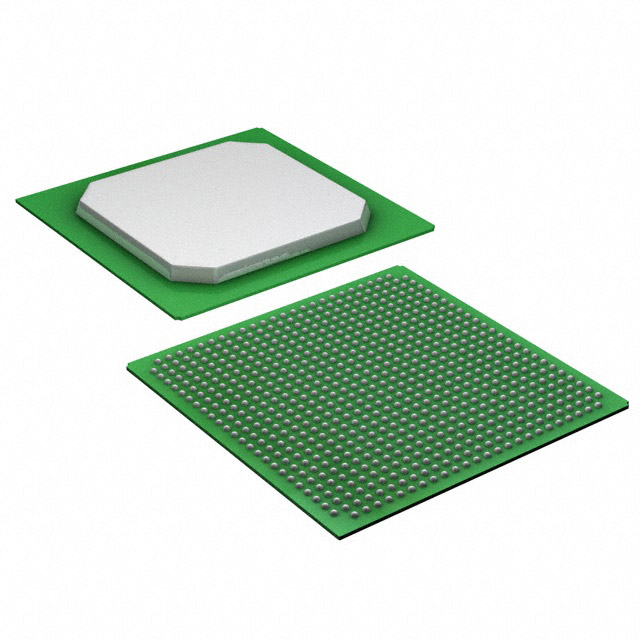
Cyclone® V GX Field Programmable Gate Array (FPGA) IC 336 14251008 301000 672-BGA |
|---|---|
| Quantity | 776 Available (as of June 18, 2026) |

| Product Category | Field Programmable Gate Array (FPGA) |
|---|---|
| Manufacturer | Intel |
| Manufacturing Status | Active |
| Manufacturer Standard Lead Time | 16 Weeks |
| Datasheet |
Specifications & Environmental
| Device Package | 672-FBGA (27x27) | Grade | Commercial | Operating Temperature | 0°C – 85°C | ||
|---|---|---|---|---|---|---|---|
| Package / Case | 672-BGA | Number of I/O | 336 | Voltage | 1.07 V - 1.13 V | ||
| Mounting Method | Surface Mount | RoHS Compliance | RoHS Compliant | REACH Compliance | REACH Unaffected | ||
| Moisture Sensitivity Level | 3 (168 Hours) | Number of LABs/CLBs | 113560 | Number of Logic Elements/Cells | 301000 | ||
| Number of Gates | N/A | ECCN | 3A001A7A | HTS Code | 8542.39.0001 | ||
| Qualification | N/A | Total RAM Bits | 14251008 |
Overview of 5CGXBC9D7F27C8N – Cyclone V GX FPGA IC, 336 I/O, 301,000 Logic Elements, 672-BGA
The 5CGXBC9D7F27C8N is an Intel Cyclone® V GX field-programmable gate array (FPGA) in a 672-ball BGA package designed for mid-density, low-power system integration. Based on the Cyclone V architecture, this device combines configurable logic, substantial embedded memory, on-chip transceivers and hard memory controller IP to address industrial, wireless/wireline and military applications that require a balanced mix of logic capacity and interfacing bandwidth.
With a core voltage around 1.1 V and a narrow supply range of 1.07 V to 1.13 V, this commercial-grade part targets designs that prioritize power efficiency and compact packaging while providing flexible I/O and embedded processing options available across the Cyclone V family.
Key Features
- Configurable Logic — 301,000 logic elements and approximately 113,560 configurable logic blocks (CLBs) provide substantial fabric capacity for custom HDL implementations and glue logic.
- Embedded Memory — Approximately 13.6 Mbits of on-chip RAM (total RAM bits: 14,251,008) for FIFOs, buffers and local storage of working datasets.
- I/O and Packaging — 336 general-purpose I/O pins in a compact 672-BGA package (supplier package: 672-FBGA, 27 × 27 mm) for dense board-level integration.
- Transceiver and System IP — Cyclone V GX series devices include integrated transceivers and hard memory controller IP; the Cyclone V family supports features such as PCIe hard IP and external memory interfaces as part of the series architecture.
- Process and Core Voltage — Built on TSMC's 28 nm low-power (28LP) process with a nominal 1.1 V core operating point; this device specifies an allowed supply range of 1.07 V to 1.13 V.
- Operating Conditions — Commercial grade with an operating temperature range of 0 °C to 85 °C and RoHS compliance for environmental adherence.
- SoC Integration Options — Cyclone V family devices include options for a hard processor system (HPS) with an integrated Arm Cortex-A9 MPCore processor in applicable variants, enabling tight processor–FPGA integration where required by the system architecture.
Typical Applications
- Industrial Automation — Motor control, sensor aggregation and machine I/O where a mix of logic, embedded memory and flexible I/O is needed for control and deterministic processing.
- Wireless and Wireline Infrastructure — PHY and protocol processing, line-rate interfacing and data-path buffering that leverage on-chip transceivers and hard memory controllers in the Cyclone V family.
- Defense and Military Systems — Signal processing and communications functions that require a combination of configurable logic capacity and embedded memory within a commercial-grade FPGA platform where specified.
- SoC and Embedded Processing — Designs that benefit from Cyclone V family HPS integration or require local FPGA acceleration alongside an external processor subsystem.
Unique Advantages
- Highly integrated FPGA fabric: 301,000 logic elements and 113,560 CLBs provide the programmable capacity to consolidate multiple discrete functions into a single device.
- Substantial on-chip memory: Approximately 13.6 Mbits of embedded memory reduces reliance on external RAM for common buffering and temporary storage tasks.
- Balanced I/O and compact footprint: 336 I/O pins in a 672-FBGA (27 × 27 mm) package enable dense board layouts without sacrificing connectivity.
- Low-voltage operation: Narrow supply window centered at 1.1 V (1.07–1.13 V) supports power-optimized system designs.
- Series-level IP and transceivers: Cyclone V GX architecture includes hard memory controllers and serial transceiver capabilities, enabling higher-bandwidth interfaces and simplified external memory connectivity in qualifying system designs.
- RoHS-compliant commercial part: Facilitates environmentally compliant procurement and assembly processes for commercial products.
Why Choose 5CGXBC9D7F27C8N?
This Cyclone V GX device balances logic density, embedded memory and I/O capability in a compact, low-voltage package suited for applications that require efficient integration of configurable logic and high-bandwidth interfaces. It is positioned for designers who need the Cyclone V family’s combination of on-chip memory, transceiver and hard-IP features without moving to higher-density or different-package variants.
Choose the 5CGXBC9D7F27C8N when you need a mid-density FPGA platform with migration-friendly package footprints, robust logic and memory resources, and commercial-grade operating parameters to support development across industrial, wireless/wireline and defense-related projects.
Request a quote or submit a procurement inquiry to start integrating the 5CGXBC9D7F27C8N into your design and evaluate availability, pricing and lead times.


Date Founded: 1968
Headquarters: Santa Clara, California, USA
Employees: 130,000+
Revenue: $54.23 Billion
Certifications and Memberships: ISO9001:2015, ISO14001:2015, ISO17025:2017, ISO27001:2022, ISO45001:2018, ISO50001:2018


