
5CGXBC9A7U19C8N
| Part Description |
Cyclone® V GX Field Programmable Gate Array (FPGA) IC 240 14251008 301000 484-FBGA |
|---|---|
| Quantity | 526 Available (as of June 15, 2026) |

| Product Category | Field Programmable Gate Array (FPGA) |
|---|---|
| Manufacturer | Intel |
| Manufacturing Status | Active |
| Manufacturer Standard Lead Time | 16 Weeks |
| Datasheet |
Specifications & Environmental
| Device Package | 484-UBGA (19x19) | Grade | Commercial | Operating Temperature | 0°C – 85°C | ||
|---|---|---|---|---|---|---|---|
| Package / Case | 484-FBGA | Number of I/O | 240 | Voltage | 1.07 V - 1.13 V | ||
| Mounting Method | Surface Mount | RoHS Compliance | RoHS Compliant | REACH Compliance | REACH Unaffected | ||
| Moisture Sensitivity Level | 3 (168 Hours) | Number of LABs/CLBs | 113560 | Number of Logic Elements/Cells | 301000 | ||
| Number of Gates | N/A | ECCN | 3A001A2C | HTS Code | 8542.39.0001 | ||
| Qualification | N/A | Total RAM Bits | 14251008 |
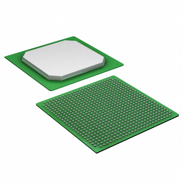
Overview of 5CGXBC9A7U19C8N – Cyclone V GX FPGA, 301000 logic elements, 484-FBGA
The 5CGXBC9A7U19C8N is an Intel Cyclone V GX field-programmable gate array (FPGA) in a 484-FBGA surface-mount package. It pairs high logic capacity with abundant on-chip memory and a broad I/O complement to implement complex custom logic, protocol bridging, and signal processing functions.
Built on TSMC's 28 nm low-power process and designed with integrated transceivers and hard memory controllers (as documented for Cyclone V GX devices), this part targets applications in industrial, wireless and wireline, and military markets that require high integration and efficient on-chip resources.
Key Features
- Core and process — Based on TSMC 28 nm low-power (28LP) process with a nominal core supply in the 1.07 V to 1.13 V range.
- Logic capacity — 301,000 logic elements and 113,560 CLBs to support large, complex designs.
- Embedded memory — Approximately 14.25 Mbits of on-chip RAM (14,251,008 bits) for buffering, LUTRAM, and local storage.
- I/O and packaging — 240 general-purpose I/O pins in a 484-FBGA (484-UBGA, 19×19) surface-mount package suitable for high-density board designs.
- Commercial operating range — Rated for operation from 0 °C to 85 °C; RoHS-compliant.
- Integrated system features — Cyclone V GX family features include integrated transceivers and hard memory controllers to simplify high-bandwidth interfaces.
Typical Applications
- Wireless and wireline communications — Protocol offload, framing, and interface bridging leveraging high logic density and integrated transceivers.
- Industrial systems — Control, data aggregation, and interface consolidation where a commercial-grade FPGA meets system requirements.
- Defense and military systems — Custom signal processing and real-time logic functions that benefit from large logic arrays and embedded memory.
- High-density I/O platforms — Applications requiring many external interfaces and compact packaging, enabled by 240 I/Os in a 19×19 BGA footprint.
Unique Advantages
- High integration density: Large logic element count and substantial on-chip RAM reduce reliance on external logic and memory, simplifying BOM and board complexity.
- Flexible I/O and interface support: 240 I/Os plus Cyclone V GX family transceiver and memory controller features enable multi-protocol designs and direct external-memory interfacing.
- Low-voltage operation: Narrow core voltage range (1.07–1.13 V) aligns with modern low-power system rails.
- Compact, manufacturable package: 484-FBGA (19×19) surface-mount package provides a balance of I/O density and board-area efficiency for volume production.
- Commercial-grade compliance: Specified for 0 °C to 85 °C operation and RoHS-compliant for standard electronic product environments.
Why Choose 5CGXBC9A7U19C8N?
This Cyclone V GX FPGA delivers a combination of high logic capacity, substantial embedded memory, and a large I/O complement in a compact 484-FBGA package. Its low-voltage 28 nm implementation and Cyclone V GX family features (integrated transceivers and memory controllers) make it suitable for designs that require on-chip resources to minimize external components while maintaining interface flexibility.
Choose 5CGXBC9A7U19C8N for mid- to high-complexity designs where commercial-grade temperature operation, high logic density, and strong on-chip memory capacity provide long-term scalability and straightforward integration into standard production flows.
Request a quote or submit an RFQ to obtain pricing and lead-time information for part number 5CGXBC9A7U19C8N.


Date Founded: 1968
Headquarters: Santa Clara, California, USA
Employees: 130,000+
Revenue: $54.23 Billion
Certifications and Memberships: ISO9001:2015, ISO14001:2015, ISO17025:2017, ISO27001:2022, ISO45001:2018, ISO50001:2018


