
5CGXFC4C6F27I7N
| Part Description |
Cyclone® V GX Field Programmable Gate Array (FPGA) IC 336 2862080 50000 672-BGA |
|---|---|
| Quantity | 154 Available (as of June 15, 2026) |
| Product Category | Field Programmable Gate Array (FPGA) |
|---|---|
| Manufacturer | Intel |
| Manufacturing Status | Active |
| Manufacturer Standard Lead Time | 12 Weeks |
| Datasheet |
Specifications & Environmental
| Device Package | 672-FBGA (27x27) | Grade | Industrial | Operating Temperature | -40°C – 100°C | ||
|---|---|---|---|---|---|---|---|
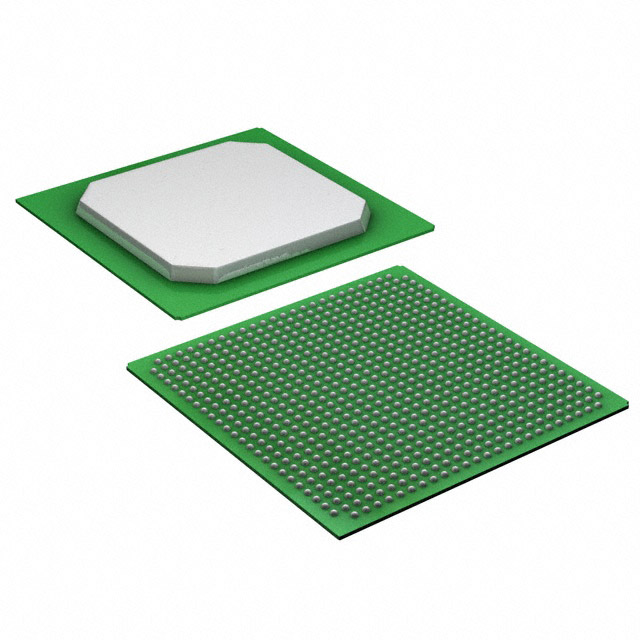
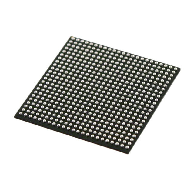
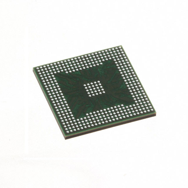
| Package / Case | 672-BGA | Number of I/O | 336 | Voltage | 1.07 V - 1.13 V | ||
| Mounting Method | Surface Mount | RoHS Compliance | RoHS Compliant | REACH Compliance | REACH Unaffected | ||
| Moisture Sensitivity Level | 3 (168 Hours) | Number of LABs/CLBs | 18868 | Number of Logic Elements/Cells | 50000 | ||
| Number of Gates | N/A | ECCN | 3A991D | HTS Code | 8542.39.0001 | ||
| Qualification | N/A | Total RAM Bits | 2862080 |
Overview of 5CGXFC4C6F27I7N – Cyclone® V GX FPGA, 50,000 Logic Elements, 672-BGA
The 5CGXFC4C6F27I7N is an Intel Cyclone V GX field-programmable gate array (FPGA) in a 672-BGA package optimized for industrial designs. It combines a mid-range logic capacity with on-chip embedded memory and a broad I/O count to support bandwidth-focused, cost-sensitive applications.
Designed for use in industrial, wireless and wireline, and military markets, this Cyclone V device family emphasizes lower power operation, integrated transceivers and hard memory controllers to address increasing bandwidth and integration requirements.
Key Features
- Logic Capacity Approximately 50,000 logic elements to implement mid-density FPGA designs.
- Embedded Memory Approximately 2.86 Mbits of embedded memory (2,862,080 bits) for on-chip buffering and storage.
- I/O 336 user I/O pins to support parallel interfaces and multiple peripheral connections.
- Transceivers and Memory IP Cyclone V family enhancements include integrated transceivers and hard memory controllers for high-bandwidth external interfaces.
- Process and Power Built on TSMC's 28-nm low-power (28LP) process technology with a core supply range of 1.07 V to 1.13 V and a typical 1.1 V core target, enabling lower overall device power consumption.
- Package and Mounting 672-BGA package (672-FBGA, 27×27) designed for surface-mount assembly.
- Operating Range Industrial-grade operation from −40 °C to 100 °C and RoHS-compliant.
Typical Applications
- Industrial Control FPGA logic and ample I/O make it suitable for motor control, PLC interfaces and sensor aggregation in industrial environments within the specified temperature range.
- Wireless and Wireline Infrastructure Integrated transceivers and hard memory controllers support high-bandwidth interface functions and protocol offload in communication equipment.
- Defense and Rugged Systems Mid-density logic, embedded memory and industrial temperature grading support signal processing and I/O-centric subsystems used in military applications.
Unique Advantages
- Balanced Mid-Range Capacity: ~50,000 logic elements provide a trade-off between density and cost for volume-sensitive designs.
- Integrated Bandwidth Features: Family-level support for integrated transceivers and hard memory controllers simplifies high-throughput interface implementations.
- Low-Power Process: TSMC 28LP-based device architecture and a narrow core voltage range help reduce system power compared with earlier generations.
- Industrial Temperature Rating: Specified operation from −40 °C to 100 °C for deployment in temperature-demanding environments.
- High I/O Count: 336 I/O pins enable flexible system partitioning and extensive peripheral connectivity without external GPIO expanders.
- Compact, Surface-Mount Package: 672-FBGA (27×27) package supports dense board layouts while maintaining robust signal routing.
Why Choose 5CGXFC4C6F27I7N?
The 5CGXFC4C6F27I7N Cyclone V GX FPGA delivers a balanced combination of logic capacity, embedded memory, and I/O resources in a surface-mount 672-BGA package suitable for industrial-class applications. Its 28-nm low-power architecture and family-level integration of transceivers and hard memory controllers help developers meet bandwidth and power targets while controlling system cost.
This device is well suited for engineers building mid-density FPGA designs that require a mix of on-chip memory, significant I/O, and industrial temperature operation, and it is supported by Intel device documentation and standard warranty provisions.
Request a quote or submit an inquiry to begin procurement and evaluate 5CGXFC4C6F27I7N for your next design.


Date Founded: 1968
Headquarters: Santa Clara, California, USA
Employees: 130,000+
Revenue: $54.23 Billion
Certifications and Memberships: ISO9001:2015, ISO14001:2015, ISO17025:2017, ISO27001:2022, ISO45001:2018, ISO50001:2018


