
5CGXFC9C7F23C8N
| Part Description |
Cyclone® V GX Field Programmable Gate Array (FPGA) IC 224 14251008 301000 484-BGA |
|---|---|
| Quantity | 631 Available (as of June 15, 2026) |

| Product Category | Field Programmable Gate Array (FPGA) |
|---|---|
| Manufacturer | Intel |
| Manufacturing Status | Active |
| Manufacturer Standard Lead Time | 16 Weeks |
| Datasheet |
Specifications & Environmental
| Device Package | 484-FBGA (23x23) | Grade | Commercial | Operating Temperature | 0°C – 85°C | ||
|---|---|---|---|---|---|---|---|
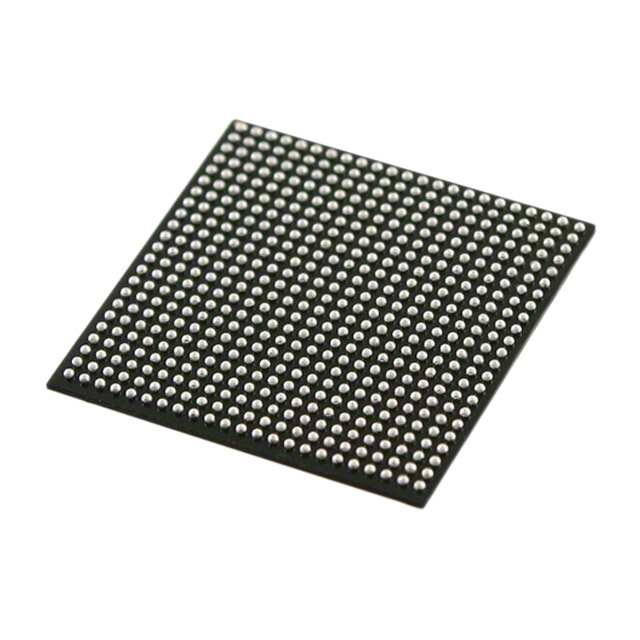
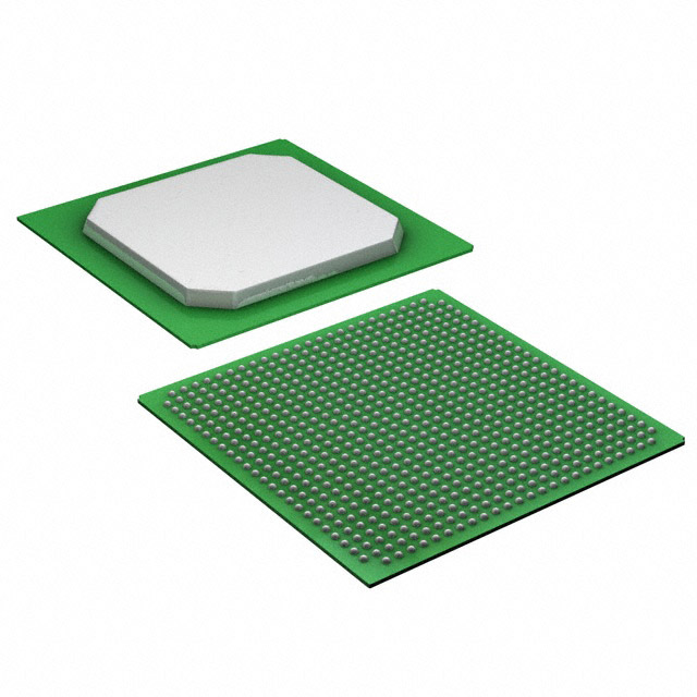
| Package / Case | 484-BGA | Number of I/O | 224 | Voltage | 1.07 V - 1.13 V | ||
| Mounting Method | Surface Mount | RoHS Compliance | RoHS Compliant | REACH Compliance | REACH Unaffected | ||
| Moisture Sensitivity Level | 3 (168 Hours) | Number of LABs/CLBs | 113560 | Number of Logic Elements/Cells | 301000 | ||
| Number of Gates | N/A | ECCN | 3A001A7A | HTS Code | 8542.39.0001 | ||
| Qualification | N/A | Total RAM Bits | 14251008 |
Overview of 5CGXFC9C7F23C8N – Cyclone® V GX Field Programmable Gate Array (FPGA) IC 224 14251008 301000 484-BGA
The 5CGXFC9C7F23C8N is a Cyclone® V GX FPGA optimized for designs that require significant programmable logic, on-chip memory, and high-speed serial interfaces. It is built on TSMC's 28‑nm low‑power (28LP) process and combines a large logic capacity with integrated transceivers and hard memory controller capabilities suitable for communications, industrial, and defense applications.
With approximately 301,000 logic elements, about 14.25 Mbits of embedded memory, and 224 I/O pins in a 484‑BGA (484‑FBGA, 23×23) package, this device targets systems that need a balance of logic density, memory, and I/O bandwidth while operating within a commercial temperature range and a tightly controlled core supply window.
Key Features
- FPGA Core — Cyclone V GX architecture implemented in TSMC 28‑nm low‑power (28LP) process; designed for reduced power consumption relative to earlier generations.
- Logic Capacity — Approximately 301,000 logic elements to handle complex programmable logic tasks and custom acceleration blocks.
- Embedded Memory — Approximately 14.25 Mbits of on‑chip RAM for large buffers, FIFOs, and embedded data structures.
- High‑Speed Serial Transceivers — Integrated transceivers supporting multi‑Gbps operation (documented transceiver options include 3.125 Gbps and 6.144 Gbps), enabling high‑bandwidth serial links.
- I/O and Packaging — 224 I/O pins in a 484‑BGA (484‑FBGA, 23×23) surface‑mount package for dense board integration and flexible external interfacing.
- Power and Voltage — Narrow core supply range of 1.07 V to 1.13 V, supporting predictable power design and regulation.
- Operating Conditions — Commercial grade device with an operating temperature range of 0 °C to 85 °C and RoHS compliance for regulatory compatibility.
- System Integration — Enhanced with hard memory controllers and on‑chip IP blocks to reduce external component count and simplify system design.
Typical Applications
- Industrial Systems — Real‑time control, motor drive interfaces, and sensor aggregation where programmable logic and on‑chip memory accelerate deterministic processing.
- Wireless and Wireline Communications — Baseband processing, fronthaul/backhaul interfacing, and high‑speed protocol bridging leveraging integrated transceivers and hard memory controllers.
- Defense and Military Electronics — Radar, signal processing, and communications subsystems that require flexible logic, embedded memory, and high‑speed serial links.
Unique Advantages
- High Logic Density: Approximately 301,000 logic elements give headroom for complex algorithms, custom accelerators, and interface logic on a single device.
- Substantial On‑Chip RAM: About 14.25 Mbits of embedded memory reduces dependence on external DRAM for many buffer and storage needs.
- Integrated High‑Speed I/O: Multi‑Gbps transceivers integrated on‑die enable compact designs with fewer external SERDES components.
- Compact, Board‑Ready Package: 484‑BGA (484‑FBGA, 23×23) surface‑mount package provides dense routing and a small board footprint for space‑constrained systems.
- Tightly Controlled Core Voltage: The 1.07–1.13 V core supply window simplifies power supply selection and helps maintain consistent performance.
- Commercial Temperature and RoHS Compliance: Suited for mainstream commercial deployments while meeting RoHS environmental requirements.
Why Choose 5CGXFC9C7F23C8N?
The 5CGXFC9C7F23C8N Cyclone V GX FPGA delivers a combination of high logic capacity, substantial embedded memory, and integrated multi‑Gbps transceivers in a compact 484‑BGA package. It is appropriate for designers who need programmable hardware acceleration, robust on‑chip storage, and high‑bandwidth I/O without moving to higher‑cost device families.
Its 28‑nm low‑power process foundation, integrated system IP (such as hard memory controllers and serial transceivers), and compatibility with established Cyclone V packaging options make it a practical choice for commercial applications in communications, industrial automation, and defense electronics where predictable supply voltage and RoHS compliance are required.
If you would like pricing, availability, or technical clarification for 5CGXFC9C7F23C8N, request a quote or submit an inquiry and our team will respond with the requested information.


Date Founded: 1968
Headquarters: Santa Clara, California, USA
Employees: 130,000+
Revenue: $54.23 Billion
Certifications and Memberships: ISO9001:2015, ISO14001:2015, ISO17025:2017, ISO27001:2022, ISO45001:2018, ISO50001:2018


