
5CGXFC9E6F31C7N
| Part Description |
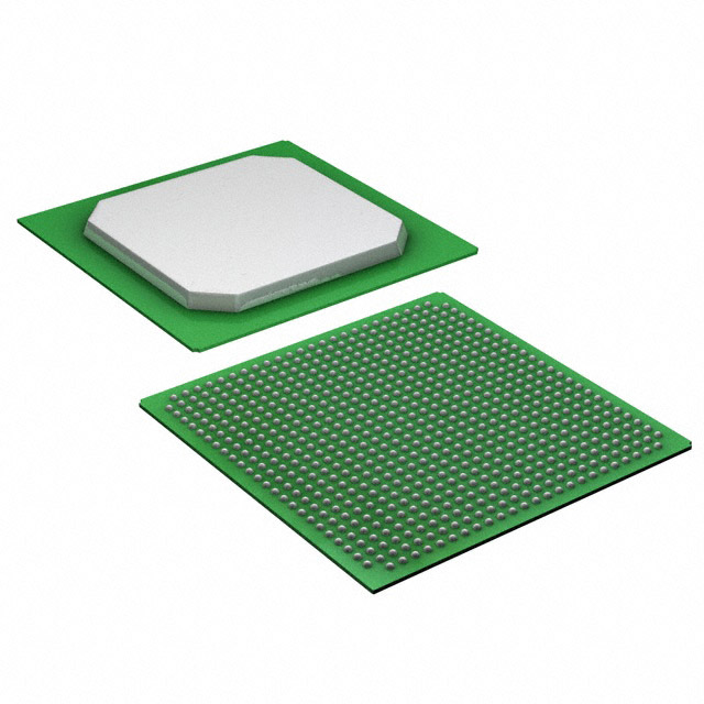
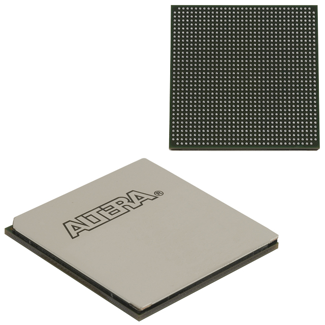
Cyclone® V GX Field Programmable Gate Array (FPGA) IC 480 14251008 301000 896-BGA |
|---|---|
| Quantity | 381 Available (as of October 7, 2026) |

| Product Category | Field Programmable Gate Array (FPGA) |
|---|---|
| Manufacturer | Intel |
| Manufacturing Status | Active |
| Manufacturer Standard Lead Time | 16 Weeks |
| Datasheet |
Specifications & Environmental
| Device Package | 896-FBGA (31x31) | Grade | Commercial | Operating Temperature | 0°C – 85°C | ||
|---|---|---|---|---|---|---|---|
| Package / Case | 896-BGA | Number of I/O | 480 | Voltage | 1.07 V - 1.13 V | ||
| Mounting Method | Surface Mount | RoHS Compliance | RoHS Compliant | REACH Compliance | REACH Unaffected | ||
| Moisture Sensitivity Level | 3 (168 Hours) | Number of LABs/CLBs | 113560 | Number of Logic Elements/Cells | 301000 | ||
| Number of Gates | N/A | ECCN | 3A001A7A | HTS Code | 8542.39.0001 | ||
| Qualification | N/A | Total RAM Bits | 14251008 |
Overview of 5CGXFC9E6F31C7N – Cyclone® V GX Field Programmable Gate Array (FPGA) IC 480 14251008 301000 896-BGA
The 5CGXFC9E6F31C7N is a Cyclone® V GX family FPGA packaged in a 896-ball BGA (896-FBGA, 31 × 31) in a surface-mount form factor. It combines a high-density programmable fabric with substantial on-chip RAM and a broad I/O count for designs that require large logic capacity, significant embedded memory, and flexible high-speed I/O.
Targeted at applications that demand integration of logic, memory and high-speed serial interfaces, this commercial-grade device delivers 301,000 logic elements, approximately 14.25 Mbits of embedded memory, and 480 general-purpose I/Os, while operating from a 1.07 V to 1.13 V core supply and across a 0 °C to 85 °C temperature range.
Key Features
- Core logic 301,000 logic elements implemented with enhanced adaptive logic modules (ALMs) for efficient logic packing and register usage.
- Embedded memory Approximately 14.25 Mbits of on-chip RAM organized in M10K memory blocks with soft error correction code (ECC) support for robust storage of intermediate data and buffers.
- DSP and processing Variable-precision DSP blocks for fixed- and floating-point signal processing; family documentation includes options for a hard processor system (HPS) with integrated Arm Cortex‑A9 for system-on-chip designs.
- I/O and high-speed serial 480 device I/Os plus integrated transceivers supporting high-speed serial rates (including 3.125 Gbps and 6.144 Gbps as documented for the Cyclone V family) for demanding communication links.
- External memory and IP Hard memory controllers and PCIe Gen1/Gen2 hard IP are available on the Cyclone V family for efficient external memory and host-interface integration.
- Power Designed on a TSMC 28-nm low-power process with a nominal core voltage near 1.1 V; operating supply window specified at 1.07 V to 1.13 V for core power planning.
- Package, mounting and environmental 896-ball FBGA (31 × 31) surface-mount package; commercial grade operation from 0 °C to 85 °C and RoHS-compliant.
Typical Applications
- Wireless and wireline communications Use the integrated high-speed transceivers and large programmable fabric for baseband processing, protocol offload, and packet handling in wired and wireless systems.
- High-bandwidth embedded systems Leverage the large logic capacity, ample on-chip RAM, and hard memory controllers for data buffering, DMA acceleration, and custom processing pipelines.
- Defense and aerospace systems Employ the device’s combination of logic density, embedded memory, and high-speed I/O for processing and I/O aggregation in mission systems where Cyclone V family devices are documented for such applications.
- SoC integration Architectures that combine FPGA fabric with an HPS (as documented for the Cyclone V family) can consolidate processor and custom logic tasks in a single silicon footprint.
Unique Advantages
- High logic density: 301,000 logic elements enable complex state machines, acceleration engines, and wide datapaths without external glue logic.
- Substantial on-chip RAM: Approximately 14.25 Mbits of embedded memory organized in M10K blocks supports large buffers, caches, and parameter storage with ECC options.
- Extensive I/O and serial capability: 480 I/Os combined with documented high-speed transceivers provide flexible interfacing to peripherals and high-throughput links.
- Low-voltage operation: Narrow core supply range (1.07–1.13 V) supports low-power design strategies and predictable power budgeting.
- Scalable SoC options: Cyclone V family documentation includes a hard processor system (HPS) option for tighter processor–FPGA integration when required by the design.
- Commercial and RoHS-compliant package: Surface-mount 896-FBGA packaging and RoHS compliance simplify assembly and environmental compliance for commercial products.
Why Choose 5CGXFC9E6F31C7N?
The 5CGXFC9E6F31C7N delivers a balanced combination of logic capacity, embedded memory, and high-speed I/O in a commercial-grade Cyclone V GX device. Its 301,000 logic elements and approximately 14.25 Mbits of RAM support complex custom logic and buffering requirements, while integrated transceivers and hard IP simplify high-bandwidth interface implementation.
This device is suitable for engineering teams building high-throughput embedded systems, communications equipment, or SoC-class designs that require substantial on-chip resources, predictable low-voltage operation, and a compact 896-FBGA package. Its family-level support for processor integration and hard memory controllers helps reduce board-level complexity and long-term BOM cost.
Request a quote or submit an inquiry to begin procurement or integration planning for the 5CGXFC9E6F31C7N.
























Date Founded: 1968
Headquarters: Santa Clara, California, USA
Employees: 130,000+
Revenue: $54.23 Billion
Certifications and Memberships: ISO9001:2015, ISO14001:2015, ISO17025:2017, ISO27001:2022, ISO45001:2018, ISO50001:2018


