
5CGXFC9E6F31I7N
| Part Description |
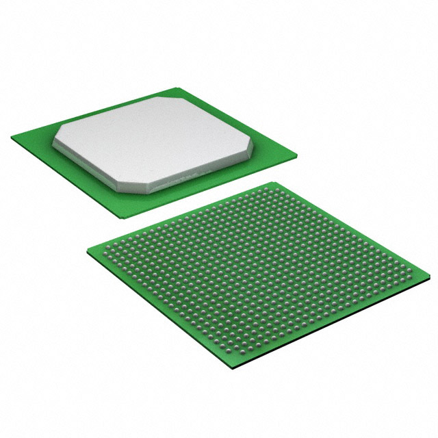
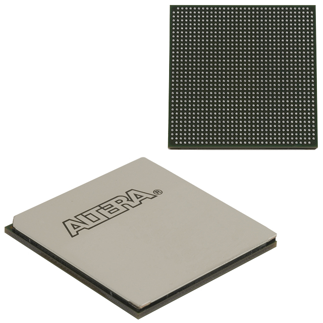
Cyclone® V GX Field Programmable Gate Array (FPGA) IC 480 14251008 301000 896-BGA |
|---|---|
| Quantity | 1,862 Available (as of October 8, 2026) |

| Product Category | Field Programmable Gate Array (FPGA) |
|---|---|
| Manufacturer | Intel |
| Manufacturing Status | Active |
| Manufacturer Standard Lead Time | 16 Weeks |
| Datasheet |
Specifications & Environmental
| Device Package | 896-FBGA (31x31) | Grade | Industrial | Operating Temperature | -40°C – 100°C | ||
|---|---|---|---|---|---|---|---|
| Package / Case | 896-BGA | Number of I/O | 480 | Voltage | 1.07 V - 1.13 V | ||
| Mounting Method | Surface Mount | RoHS Compliance | RoHS Compliant | REACH Compliance | REACH Unaffected | ||
| Moisture Sensitivity Level | 3 (168 Hours) | Number of LABs/CLBs | 113560 | Number of Logic Elements/Cells | 301000 | ||
| Number of Gates | N/A | ECCN | 3A991D | HTS Code | 8542.39.0001 | ||
| Qualification | N/A | Total RAM Bits | 14251008 |
Overview of 5CGXFC9E6F31I7N – Cyclone® V GX FPGA, 301,000 Logic Elements, 480 I/O, 896‑BGA
The 5CGXFC9E6F31I7N is an Intel Cyclone® V GX field programmable gate array (FPGA) IC designed for high-density, cost-sensitive systems. This device integrates a large FPGA fabric with transceiver and memory-focused features suitable for industrial, wireless and wireline communications, and military applications.
With 301,000 logic elements, approximately 14.25 Mbits of embedded memory, and 480 general‑purpose I/O, this 896‑ball BGA, surface‑mount device delivers a balance of logic capacity, I/O density, and system integration for complex embedded designs operating across a wide temperature range.
Key Features
- High-density logic — 301,000 logic elements provide significant programmable fabric for complex logic, control, and signal processing tasks.
- Embedded memory — Approximately 14.25 Mbits of on‑chip RAM to support large buffer, lookup, and state storage requirements without immediate external memory dependence.
- I/O and package — 480 I/O pins in a 896‑BGA (896‑FBGA, 31×31) surface‑mount package, enabling high‑pin‑count peripheral interfacing and board routing flexibility.
- Voltage and power — Core supply range of 1.07 V to 1.13 V to meet system power rails and enable predictable power budgeting.
- Industrial temperature rating — Specified operating range from −40°C to 100°C for reliable deployment in industrial environments.
- Integrated hard IP and transceivers — Family-level features include integrated transceivers and hard memory controller IP, supporting high‑bandwidth interfaces and simplified system integration.
- RoHS compliant — Meets environmental compliance requirements for lead‑free assembly and manufacturing.
Typical Applications
- Industrial control — Programmable logic and abundant I/O make it suitable for motion control, PLC augmentation, and real‑time signal aggregation in industrial systems.
- Wireless and wireline communications — Integrated transceiver capabilities and large logic/memory resources support protocol processing, fronthaul/backhaul functions, and data aggregation.
- Defense and test equipment — Industrial temperature rating and high logic density enable custom processing, I/O conditioning, and protocol bridging in ruggedized test and defense electronics.
- Embedded compute and acceleration — On‑chip memory and extensive logic resources allow for hardware acceleration of algorithms, packet processing, and sensor fusion tasks.
Unique Advantages
- Large programmable capacity: 301,000 logic elements let you map complex state machines, DSP pipelines, and control logic without immediate external FPGA expansion.
- Substantial on‑chip memory: Approximately 14.25 Mbits of embedded RAM reduces dependency on external memory for buffering and accelerates data‑path designs.
- High I/O count in a compact package: 480 I/Os in an 896‑FBGA (31×31) package provides dense routing for multi‑lane interfaces and peripheral connectivity.
- Industrial temperature range: −40°C to 100°C operation supports deployments in demanding environmental conditions common to industrial and defense applications.
- System integration through hard IP: Family‑level hard IP and transceiver integration simplify implementation of high‑bandwidth interfaces and reduce overall system BOM.
- Predictable power envelope: Defined core supply range (1.07–1.13 V) helps in designing stable power delivery and thermal solutions.
Why Choose 5CGXFC9E6F31I7N?
The 5CGXFC9E6F31I7N targets designs that require a high logic count, substantial embedded memory, and a large number of I/O in a single, surface‑mount FPGA package rated for industrial environments. Its combination of programmable capacity, on‑chip RAM, and integrated system IP supports efficient implementation of communication, control, and embedded acceleration functions while helping to contain BOM and board complexity.
This device is well suited to engineering teams building ruggedized, bandwidth‑oriented systems that need a scalable FPGA foundation backed by documented family‑level features and environmental compliance.
Request a quote or submit a purchase inquiry to get pricing and availability for the 5CGXFC9E6F31I7N. Provide your project requirements and quantity to receive a prompt response.
























Date Founded: 1968
Headquarters: Santa Clara, California, USA
Employees: 130,000+
Revenue: $54.23 Billion
Certifications and Memberships: ISO9001:2015, ISO14001:2015, ISO17025:2017, ISO27001:2022, ISO45001:2018, ISO50001:2018


