
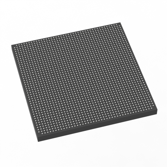
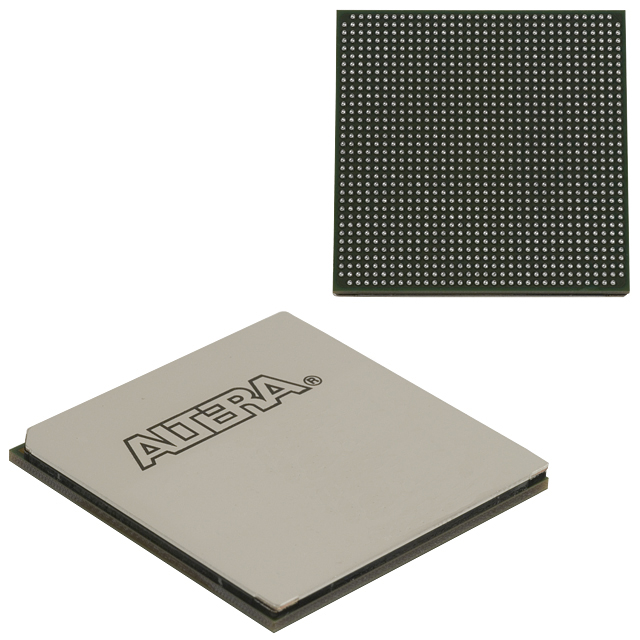
5CGXFC9E7F31C8N
| Part Description |
Cyclone® V GX Field Programmable Gate Array (FPGA) IC 480 14251008 301000 896-BGA |
|---|---|
| Quantity | 842 Available (as of June 15, 2026) |

| Product Category | Field Programmable Gate Array (FPGA) |
|---|---|
| Manufacturer | Intel |
| Manufacturing Status | Active |
| Manufacturer Standard Lead Time | 16 Weeks |
| Datasheet |
Specifications & Environmental
| Device Package | 896-FBGA (31x31) | Grade | Commercial | Operating Temperature | 0°C – 85°C | ||
|---|---|---|---|---|---|---|---|
| Package / Case | 896-BGA | Number of I/O | 480 | Voltage | 1.07 V - 1.13 V | ||
| Mounting Method | Surface Mount | RoHS Compliance | RoHS Compliant | REACH Compliance | REACH Unaffected | ||
| Moisture Sensitivity Level | 3 (168 Hours) | Number of LABs/CLBs | 113560 | Number of Logic Elements/Cells | 301000 | ||
| Number of Gates | N/A | ECCN | 3A001A7A | HTS Code | 8542.39.0001 | ||
| Qualification | N/A | Total RAM Bits | 14251008 |
Overview of 5CGXFC9E7F31C8N – Cyclone® V GX Field Programmable Gate Array (FPGA) IC 480 14251008 301000 896-BGA
The 5CGXFC9E7F31C8N is a Cyclone® V GX FPGA in an 896-ball BGA (31×31) package designed for cost-sensitive, bandwidth-driven applications. It combines a large FPGA fabric with abundant I/O and embedded memory to support system functions that require programmable logic, flexible I/O, and on-chip storage.
From communications and wireless infrastructure to industrial and military system designs, the device targets applications that benefit from integrated transceivers and hard memory controllers as part of the Cyclone V device family.
Key Features
- Logic Capacity — 301,000 logic elements and 113,560 logic modules provide ample programmable fabric for complex control, signal processing, and glue-logic tasks.
- Embedded Memory — Approximately 14.25 Mbits of embedded memory (14,251,008 bits) for FIFOs, line buffers, and on-chip data storage to reduce external memory dependency.
- I/O Count — 480 user I/O pins to support wide parallel interfaces, multiple memory buses, and diverse peripheral connections.
- Package & Mounting — 896-ball FBGA (31 × 31) in a surface-mount package for compact board integration and scalable board-level routing.
- Power — Core supply specified between 1.07 V and 1.13 V (nominal 1.1 V), matching low-voltage system rails for efficient power distribution.
- Operating Range — Commercial temperature range from 0 °C to 85 °C for standard industrial-environment electronics.
- Process & Core — Built on a 28 nm low-power process with a 1.1 V core (Cyclone V family characteristic), enabling reduced power consumption for volume-sensitive designs.
Typical Applications
- Wireless Infrastructure — Implement protocol processing, baseband offload, or interface bridging using the device’s large logic count and integrated transceiver support.
- Wireline Communications — Use the available I/O and embedded memory for packet buffering, protocol adaptation, and custom line-rate logic.
- Industrial Control — Deploy for motor control, sensor aggregation, and deterministic control logic where large on-chip memory and numerous I/Os simplify system design.
- Military Systems — Leverage the configurable logic and on-chip resources for custom signal processing and interface consolidation in defense applications.
Unique Advantages
- High Logic Density: 301,000 logic elements enable integration of multiple subsystems into a single FPGA, reducing external components and PCB complexity.
- Substantial On-Chip Memory: Approximately 14.25 Mbits of embedded memory supports buffering and local data storage to improve system throughput and latency.
- Extensive I/O: 480 I/Os permit broad peripheral connectivity and parallel bus implementations without external multiplexing hardware.
- Compact Packaging: 896-FBGA (31×31) surface-mount package balances pin count and board-area efficiency for high-density designs.
- Low-Voltage Core: Narrow core supply range (1.07–1.13 V) simplifies power-supply design for systems using 1.1 V rails.
- Commercial Temperature Range: Rated 0 °C to 85 °C for mainstream electronic products and typical deployment environments.
Why Choose 5CGXFC9E7F31C8N?
This Cyclone V GX FPGA delivers a balanced combination of programmable logic capacity, embedded memory, and extensive I/O in a compact 896-ball FBGA package. It is suited to designs that require on-chip buffering, flexible interface support, and significant logic integration while maintaining a commercial temperature profile and low-voltage core operation.
For engineering teams building communications, industrial control, or defense systems, the 5CGXFC9E7F31C8N offers scalability across the Cyclone V family and on-chip resources that help reduce BOM cost and board-level complexity.
Request a quote or submit a procurement inquiry to obtain pricing, availability, and lead-time information for part number 5CGXFC9E7F31C8N.


Date Founded: 1968
Headquarters: Santa Clara, California, USA
Employees: 130,000+
Revenue: $54.23 Billion
Certifications and Memberships: ISO9001:2015, ISO14001:2015, ISO17025:2017, ISO27001:2022, ISO45001:2018, ISO50001:2018


