
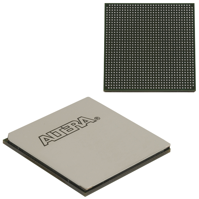
5CGXFC9E7F35C8N
| Part Description |
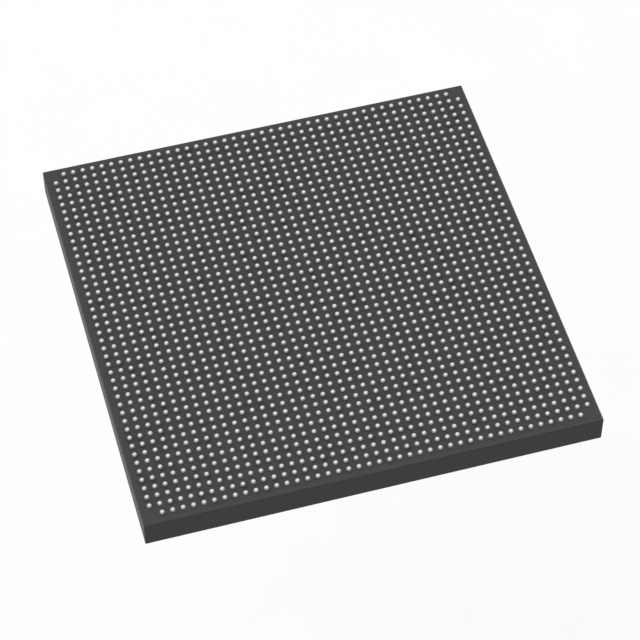
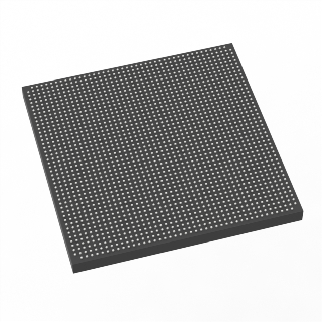
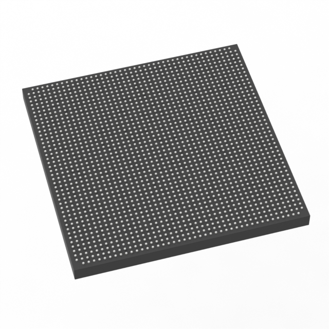
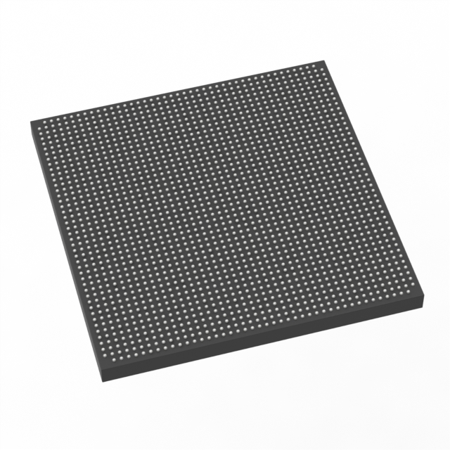
Cyclone® V GX Field Programmable Gate Array (FPGA) IC 560 14251008 301000 1152-BGA |
|---|---|
| Quantity | 387 Available (as of October 8, 2026) |

| Product Category | Field Programmable Gate Array (FPGA) |
|---|---|
| Manufacturer | Intel |
| Manufacturing Status | Active |
| Manufacturer Standard Lead Time | 16 Weeks |
| Datasheet |
Specifications & Environmental
| Device Package | 1152-FBGA (35x35) | Grade | Commercial | Operating Temperature | 0°C – 85°C | ||
|---|---|---|---|---|---|---|---|
| Package / Case | 1152-BGA | Number of I/O | 560 | Voltage | 1.07 V - 1.13 V | ||
| Mounting Method | Surface Mount | RoHS Compliance | RoHS Compliant | REACH Compliance | REACH Unaffected | ||
| Moisture Sensitivity Level | 3 (168 Hours) | Number of LABs/CLBs | 113560 | Number of Logic Elements/Cells | 301000 | ||
| Number of Gates | N/A | ECCN | 3A001A7A | HTS Code | 8542.39.0001 | ||
| Qualification | N/A | Total RAM Bits | 14251008 |
Overview of 5CGXFC9E7F35C8N – Cyclone® V GX Field Programmable Gate Array (FPGA) IC 560 14251008 301000 1152-BGA
The 5CGXFC9E7F35C8N is a Cyclone® V GX FPGA in a 1152-BGA (35×35) package, offering a high-density programmable fabric targeted at cost-sensitive, high-volume designs. It combines a large logic capacity, embedded memory, and extensive I/O to address applications in industrial systems, wireless and wireline communications, and military markets.
Built on the Cyclone V family architecture and implemented in a low-power 28 nm process, this device delivers integration and power-efficiency advantages through integrated transceivers and hard memory controller capabilities while operating from a core supply range of 1.07 V to 1.13 V.
Key Features
- Logic Capacity — 301,000 logic elements for implementing complex digital functions and custom accelerators.
- Embedded Memory — Approximately 14.25 Mbits of on-chip RAM to support buffering, FIFOs, and local data storage.
- I/O Density — 560 user I/O pins to interface with multiple peripherals, memory devices, and high-pin-count ecosystems.
- Packaging & Mounting — 1152-FBGA (35×35) package in a surface-mount form factor suitable for compact board layouts.
- Power — Core supply range of 1.07 V to 1.13 V with a nominal 1.1 V core voltage as defined for the Cyclone V family, enabling low-power operation.
- Operating Conditions — Commercial-grade operation from 0 °C to 85 °C.
- Process & FPGA Fabric — Based on TSMC 28‑nm low-power (28LP) process technology and the Cyclone V device architecture, including enhanced adaptive logic modules and DSP resources.
- Integrated System Features — Cyclone V family capabilities include integrated transceivers, hard memory controllers, and support for advanced configuration features such as dynamic and partial reconfiguration.
- Compliance — RoHS compliant for regulatory environmental requirements.
Typical Applications
- Wireless and Wireline Communications — Implement high-speed transceiver interfaces and packet processing functions using the device’s integrated transceiver and logic capacity.
- External Memory Interfaces — Use the embedded memory and hard memory controller support for bridging and buffering between processors and external DRAM.
- Industrial Systems — Enable deterministic control, sensor aggregation, and protocol bridging in automation and machine-control applications.
- Defense and Aerospace Systems — Support complex signal processing and custom logic implementations where integration and I/O density are required.
Unique Advantages
- High integration density: 301,000 logic elements and approximately 14.25 Mbits of embedded RAM reduce the need for external logic and memory, simplifying board-level BOMs.
- Broad I/O capability: 560 I/O pins enable connection to multiple high-speed interfaces, sensors, and memory devices without external expanders.
- Low-power silicon: Implemented on a 28 nm low-power process and operating around a 1.1 V core range to help reduce system power consumption.
- Compact, manufacturable package: 1152-FBGA (35×35) surface-mount package supports dense PCB layouts for space-constrained designs.
- Design flexibility: Cyclone V family features such as adaptive logic modules, embedded memory blocks, DSP resources, and configuration options enable a wide range of custom hardware accelerators and interfaces.
Why Choose 5CGXFC9E7F35C8N?
The 5CGXFC9E7F35C8N combines substantial logic and memory capacity with a high I/O count and a compact 1152‑BGA footprint, making it well suited for designs that require integration of complex digital processing, high-bandwidth interfaces, and extensive external connectivity. Its implementation on 28 nm low-power technology and support for Cyclone V family system features balance performance with power efficiency.
This device is aimed at engineering teams designing cost-sensitive, high-volume products that need a commercially graded FPGA with robust integration options—delivering scalability, reliable supply-chain packaging, and a feature set aligned with communications, industrial, and defense applications.
Request a quote or submit a procurement inquiry to evaluate 5CGXFC9E7F35C8N for your next design. Technical and purchasing teams can provide pricing, availability, and sample options.























Date Founded: 1968
Headquarters: Santa Clara, California, USA
Employees: 130,000+
Revenue: $54.23 Billion
Certifications and Memberships: ISO9001:2015, ISO14001:2015, ISO17025:2017, ISO27001:2022, ISO45001:2018, ISO50001:2018


