
5SEE9F45C2LN
| Part Description |
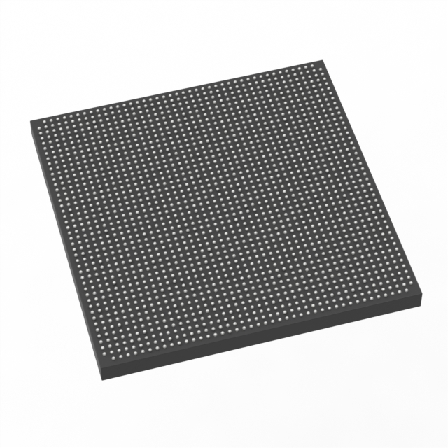
Stratix® V E Field Programmable Gate Array (FPGA) IC 840 53248000 840000 1932-BBGA, FCBGA |
|---|---|
| Quantity | 798 Available (as of June 10, 2026) |
| Product Category | Field Programmable Gate Array (FPGA) |
|---|---|
| Manufacturer | Intel |
| Manufacturing Status | Obsolete |
| Manufacturer Standard Lead Time | Contact Us |
| Datasheet |
Specifications & Environmental
| Device Package | 1932-FBGA, FC (45x45) | Grade | Commercial | Operating Temperature | 0°C – 85°C | ||
|---|---|---|---|---|---|---|---|
| Package / Case | 1932-BBGA, FCBGA | Number of I/O | 840 | Voltage | 820 mV - 880 mV | ||
| Mounting Method | Surface Mount | RoHS Compliance | RoHS Compliant | REACH Compliance | REACH Unknown | ||
| Moisture Sensitivity Level | 3 (168 Hours) | Number of LABs/CLBs | 317000 | Number of Logic Elements/Cells | 840000 | ||
| Number of Gates | N/A | ECCN | 3A001A2C | HTS Code | 8542.39.0001 | ||
| Qualification | N/A | Total RAM Bits | 53248000 |
Overview of 5SEE9F45C2LN – Stratix® V E FPGA IC, 840,000 logic elements, 1932‑BBGA (FCBGA)
The 5SEE9F45C2LN is an Intel Stratix® V E field programmable gate array (FPGA) offering high logic density and extensive on‑chip memory for demanding digital designs. Built on the Stratix V architecture, this E‑variant device is targeted at applications that require large programmable fabric capacity and advanced hard IP integration.
With 840,000 logic elements, approximately 53.25 Mbits of embedded memory, and up to 840 I/Os in a 1932‑BBGA FCBGA package, this device is suited to system emulation, diagnostic imaging, instrumentation, and other data‑intensive use cases where integration and capacity matter.
Key Features
- High Logic Density — 840,000 logic elements to implement large, complex designs and system-level prototypes.
- Embedded Memory — Approximately 53.25 Mbits of on‑chip RAM (total RAM bits: 53,248,000) for buffering, tables, and on‑chip data storage.
- I/O Capacity — Up to 840 I/O pins to support rich peripheral and high‑channel-count interfacing.
- Stratix V Architecture — Family features include a redesigned adaptive logic module (ALM), 20‑Kbit M20K embedded memory blocks, variable‑precision DSP blocks, fractional PLLs, and Embedded HardCopy blocks for hardened IP instantiation.
- Power and Supply — Core voltage supply specified between 820 mV and 880 mV to align with the Stratix V device core requirements.
- Package and Mounting — 1932‑BBGA FCBGA package (supplier package: 1932‑FBGA, FC 45×45) designed for surface‑mount assembly.
- Commercial Grade — Rated for operation from 0 °C to 85 °C; RoHS compliant.
Typical Applications
- ASIC and System Emulation — Use the large programmable fabric to prototype and validate ASIC and complex system designs before production.
- Diagnostic Imaging — High logic density and substantial embedded RAM make the device suitable for real‑time image processing pipelines and algorithm acceleration.
- Instrumentation — Integrate multi‑channel processing, custom measurement logic, and control functions in a single FPGA package.
- Data‑Intensive DSP and Networking — Family characteristics support high‑precision DSP workloads and data‑centric applications such as high‑throughput packet processing.
Unique Advantages
- Large On‑Chip Capacity: 840,000 logic elements and ~53.25 Mbits of embedded memory enable consolidation of functions and reduction of external components.
- Rich FPGA Fabric: Stratix V family features such as redesigned ALMs, M20K memory blocks, DSP blocks, and fractional PLLs provide flexible building blocks for complex designs.
- Extensive I/O: Up to 840 I/Os support dense system integration and interfacing with multiple peripherals or high‑channel systems.
- Package Density: 1932‑BBGA FCBGA provides high pin count in a compact footprint for board‑level density and performance.
- Commercial Temperature Rating: 0 °C to 85 °C operation suitable for standard commercial products and systems.
- Compliance and Assembly: Surface‑mount package with RoHS compliance simplifies procurement and manufacturing workflows.
Why Choose 5SEE9F45C2LN?
The 5SEE9F45C2LN positions itself as a high‑capacity Stratix V E device for designers who need significant programmable logic, substantial embedded memory, and broad I/O capability in a single FPGA package. It is especially appropriate for teams developing system emulation, diagnostic imaging, instrumentation, or other data‑intensive applications where integration and scalable prototyping are priorities.
Choosing this Stratix V E part provides access to the Stratix V family architecture and its hard IP blocks, enabling a development path that can scale toward production options offered by the vendor. The combination of logic density, memory, I/O, and package density delivers a practical platform for complex, integration‑centric systems.
Request a quote or submit a product inquiry to get pricing and availability for part number 5SEE9F45C2LN.


Date Founded: 1968
Headquarters: Santa Clara, California, USA
Employees: 130,000+
Revenue: $54.23 Billion
Certifications and Memberships: ISO9001:2015, ISO14001:2015, ISO17025:2017, ISO27001:2022, ISO45001:2018, ISO50001:2018


