
5SGSED8N2F45I2
| Part Description |
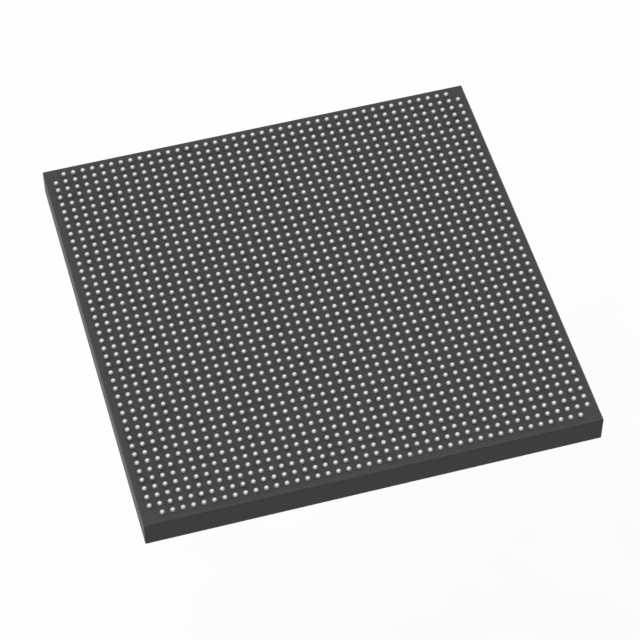
Stratix® V GS Field Programmable Gate Array (FPGA) IC 840 51200000 695000 1932-BBGA, FCBGA |
|---|---|
| Quantity | 1,455 Available (as of June 10, 2026) |

| Product Category | Field Programmable Gate Array (FPGA) |
|---|---|
| Manufacturer | Intel |
| Manufacturing Status | Obsolete |
| Manufacturer Standard Lead Time | Contact Us |
| Datasheet |
Specifications & Environmental
| Device Package | 1932-FBGA, FC (45x45) | Grade | Industrial | Operating Temperature | -40°C – 100°C | ||
|---|---|---|---|---|---|---|---|
| Package / Case | 1932-BBGA, FCBGA | Number of I/O | 840 | Voltage | 870 mV - 930 mV | ||
| Mounting Method | Surface Mount | RoHS Compliance | RoHS Compliant | REACH Compliance | REACH Unknown | ||
| Moisture Sensitivity Level | 3 (168 Hours) | Number of LABs/CLBs | 262400 | Number of Logic Elements/Cells | 695000 | ||
| Number of Gates | N/A | ECCN | 3A001A2C | HTS Code | 8542.39.0001 | ||
| Qualification | N/A | Total RAM Bits | 51200000 |
Overview of 5SGSED8N2F45I2 – Stratix® V GS FPGA, 695,000 logic elements
The 5SGSED8N2F45I2 is an Intel Stratix® V GS field-programmable gate array provided in a 1932-BBGA FCBGA package. It combines high logic density with abundant embedded memory and transceiver/DSP-oriented architecture to support bandwidth- and signal-processing-centric designs.
Targeted at industrial applications, this device offers a large I/O count, a broad operating temperature range, and a low core-voltage supply window to meet demanding system requirements for communications, DSP, and high-performance computing workloads.
Key Features
- Logic Capacity 695,000 logic elements and 262,400 LABs provide substantial programmable fabric for complex logic and control systems.
- On‑Chip Memory Approximately 51.2 Mbits of embedded memory (total RAM bits: 51,200,000) for buffering, lookup tables, and data storage within designs.
- DSP and Transceiver‑Oriented Architecture Stratix V GS family architecture includes variable-precision DSP resources and integrated transceivers tailored for transceiver-based, DSP-centric applications.
- I/O Density 840 user I/Os to support wide external interfacing, high-pin-count peripherals, and complex board-level connectivity.
- Power and Voltage Core supply range of 870 mV to 930 mV to match platform power requirements and system power-management approaches.
- Package and Mounting 1932-BBGA (FCBGA) supplier device package 1932-FBGA, FC (45×45) in a surface-mount form factor for dense board integration.
- Industrial Temperature Range Rated for operation from −40 °C to 100 °C to meet industrial-environment deployment needs.
- Compliance RoHS-compliant manufacturing to meet regulatory and environmental requirements.
Typical Applications
- High‑performance DSP systems Leverage the device’s DSP‑oriented architecture and substantial logic element count for intensive signal processing and algorithm acceleration.
- Backplane and optical communications Use integrated transceiver‑capable architecture and high I/O density for packet processing, transport, and interface bridging.
- Network and compute appliances Implement complex packet management, traffic shaping, and custom offload logic using the large programmable fabric and embedded memory.
- Industrial systems Deploy in industrial control, instrumentation, and broadcast equipment that require extended temperature operation and high integration.
Unique Advantages
- High logic density: 695,000 logic elements enable implementation of large, complex designs without partitioning across multiple devices.
- Significant on‑chip memory: Approximately 51.2 Mbits of embedded RAM reduces dependence on external memory for many buffering and caching needs.
- Rich I/O resources: 840 I/Os provide flexibility for multi-channel interfaces and dense board-level connectivity.
- Designed for DSP workloads: GS family architecture and variable‑precision DSP resources support high-precision and high-throughput signal processing tasks.
- Industrial readiness: Surface-mount 1932-BBGA package and −40 °C to 100 °C operating range match many industrial deployment requirements.
- Controlled core supply: Narrow supply window (870–930 mV) supports predictable power provisioning and thermal planning.
Why Choose 5SGSED8N2F45I2?
The 5SGSED8N2F45I2 brings the Stratix V GS family’s DSP- and transceiver-oriented architecture together with substantial logic and memory resources in a single 1932-BBGA package. Its combination of 695,000 logic elements, approximately 51.2 Mbits of embedded memory, and 840 I/Os makes it well suited for communications, high‑performance signal processing, and industrial compute applications where integration and throughput matter.
With an industrial operating temperature range and RoHS compliance, this device provides a production-ready option for engineers seeking a high-density, high-capacity FPGA platform backed by Stratix V family design resources.
If you would like pricing or availability for 5SGSED8N2F45I2, request a quote or submit an inquiry to receive a prompt response from our team.


Date Founded: 1968
Headquarters: Santa Clara, California, USA
Employees: 130,000+
Revenue: $54.23 Billion
Certifications and Memberships: ISO9001:2015, ISO14001:2015, ISO17025:2017, ISO27001:2022, ISO45001:2018, ISO50001:2018


