
5SGSED8N3F45C2N
| Part Description |
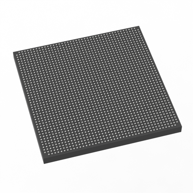
Stratix® V GS Field Programmable Gate Array (FPGA) IC 840 51200000 695000 1932-BBGA, FCBGA |
|---|---|
| Quantity | 931 Available (as of June 15, 2026) |

| Product Category | Field Programmable Gate Array (FPGA) |
|---|---|
| Manufacturer | Intel |
| Manufacturing Status | Obsolete |
| Manufacturer Standard Lead Time | Contact Us |
| Datasheet |
Specifications & Environmental
| Device Package | 1932-FBGA, FC (45x45) | Grade | Commercial | Operating Temperature | 0°C – 85°C | ||
|---|---|---|---|---|---|---|---|
| Package / Case | 1932-BBGA, FCBGA | Number of I/O | 840 | Voltage | 870 mV - 930 mV | ||
| Mounting Method | Surface Mount | RoHS Compliance | RoHS Compliant | REACH Compliance | REACH Unknown | ||
| Moisture Sensitivity Level | 3 (168 Hours) | Number of LABs/CLBs | 262400 | Number of Logic Elements/Cells | 695000 | ||
| Number of Gates | N/A | ECCN | 3A001A2C | HTS Code | 8542.39.0001 | ||
| Qualification | N/A | Total RAM Bits | 51200000 |
Overview of 5SGSED8N3F45C2N – Stratix® V GS Field Programmable Gate Array (FPGA) IC, 840 I/O, ~695,000 Logic Elements
The 5SGSED8N3F45C2N is a Stratix V GS family FPGA in a 1932-BBGA FCBGA package, designed for DSP-centric and transceiver-based designs. Built on the Stratix V architecture, the device targets high-density logic, large embedded memory, and extensive I/O for data-intensive applications.
This commercial-grade part offers a combination of high logic capacity, significant on-chip RAM, and a low-voltage core supply range, making it suitable for demanding signal processing, networking, and compute-accelerated workloads.
Key Features
- Logic Capacity — 695,000 logic elements, enabling complex designs and high integration density.
- Embedded Memory — Approximately 51.2 Mbits of on-chip RAM (51,200,000 bits total) for buffering, packet storage, and fast local data access.
- I/O Density — 840 I/O pins to support wide parallel interfaces and high-pin-count connectivity.
- Package and Mounting — 1932-BBGA (FCBGA) package, supplier device package 1932-FBGA, FC (45×45); surface-mount mounting type for board-level assembly.
- Power and Voltage — Core voltage supply specified from 870 mV to 930 mV, aligning with low-voltage 28-nm FPGA core operation.
- Operating Range — Commercial grade with an operating temperature range of 0 °C to 85 °C.
- Family-Level Architecture — Stratix V family features such as redesigned adaptive logic modules (ALMs), M20K embedded memory blocks, variable-precision DSP resources, fractional PLLs, and integrated hard IP blocks are part of the device architecture.
- Transceiver and DSP Orientation — As a GS variant in the Stratix V family, the device is positioned for transceiver-enabled, DSP-centric applications (family-level transceiver and DSP capabilities described in the Stratix V documentation).
- Compliance — RoHS compliant.
Typical Applications
- High-Performance DSP — Large logic fabric and substantial embedded memory make the device suitable for compute-heavy signal processing tasks and algorithm acceleration.
- Networking and Packet Processing — High I/O count and on-chip RAM support buffering and interface handling for data-path and packet-processing functions.
- Broadcast and Communications — GS-family orientation toward transceiver-enabled DSP makes it applicable to broadcast, wireline, and optical interface processing.
- High-Performance Computing — Dense logic and memory resources support custom accelerators and offload functions in compute systems.
Unique Advantages
- High Logic Density: 695,000 logic elements enable consolidation of complex functions and high integration on a single device, reducing system BOM and board area.
- Substantial On-Chip Memory: Approximately 51.2 Mbits of embedded RAM provides accessible local storage for high-throughput buffering and state retention.
- Extensive I/O Count: 840 I/Os accommodate wide parallel interfaces, multiple protocol endpoints, and flexible board-level connectivity options.
- Low-Voltage Core Operation: Core supply range of 0.87 V–0.93 V supports the Stratix V low-voltage architecture for efficient power use at scale.
- Robust Packaging: 1932-BBGA (FCBGA) package supports high-pin-count routing and reliable surface-mount assembly for production systems.
- Proven Family Architecture: Leveraging Stratix V family features (ALMs, M20K memory, variable-precision DSP, fractional PLLs, and embedded hard IP) provides a development path using established FPGA building blocks.
Why Choose 5SGSED8N3F45C2N?
The 5SGSED8N3F45C2N delivers a balanced combination of high logic capacity, significant on-chip memory, and a large I/O count in a production-ready FCBGA package. Its commercial temperature rating and low-voltage core operation suit system designs that require dense FPGA logic and memory resources for DSP, networking, and compute-acceleration tasks.
This device is appropriate for engineers and teams building transceiver-enabled, DSP-focused systems who need a scalable FPGA fabric with extensive I/O and embedded memory, supported by the Stratix V family architecture.
Request a quote or submit an inquiry to obtain pricing and availability for the 5SGSED8N3F45C2N.


Date Founded: 1968
Headquarters: Santa Clara, California, USA
Employees: 130,000+
Revenue: $54.23 Billion
Certifications and Memberships: ISO9001:2015, ISO14001:2015, ISO17025:2017, ISO27001:2022, ISO45001:2018, ISO50001:2018


