
5SGSED8N3F45C3N
| Part Description |
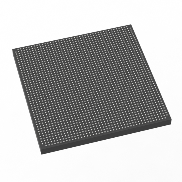
Stratix® V GS Field Programmable Gate Array (FPGA) IC 840 51200000 695000 1932-BBGA, FCBGA |
|---|---|
| Quantity | 530 Available (as of June 15, 2026) |

| Product Category | Field Programmable Gate Array (FPGA) |
|---|---|
| Manufacturer | Intel |
| Manufacturing Status | Obsolete |
| Manufacturer Standard Lead Time | Contact Us |
| Datasheet |
Specifications & Environmental
| Device Package | 1932-FBGA, FC (45x45) | Grade | Commercial | Operating Temperature | 0°C – 85°C | ||
|---|---|---|---|---|---|---|---|
| Package / Case | 1932-BBGA, FCBGA | Number of I/O | 840 | Voltage | 820 mV - 880 mV | ||
| Mounting Method | Surface Mount | RoHS Compliance | RoHS Compliant | REACH Compliance | REACH Unknown | ||
| Moisture Sensitivity Level | 3 (168 Hours) | Number of LABs/CLBs | 262400 | Number of Logic Elements/Cells | 695000 | ||
| Number of Gates | N/A | ECCN | 3A001A2C | HTS Code | 8542.39.0001 | ||
| Qualification | N/A | Total RAM Bits | 51200000 |
Overview of 5SGSED8N3F45C3N – Stratix® V GS Field Programmable Gate Array (FPGA) IC
The 5SGSED8N3F45C3N is an Intel Stratix V GS series FPGA built on a 28‑nm process. It combines high logic and memory capacity with integrated transceivers and variable‑precision DSP resources, targeting transceiver‑based, DSP‑centric and high‑bandwidth designs.
This device is optimized for bandwidth‑ and data‑intensive applications where large on‑chip memory, extensive I/O and high logic density are required. Its package and power characteristics support surface‑mount deployment in commercial‑grade systems.
Key Features
- Core & process 28‑nm TSMC process technology with Stratix V architecture elements including redesigned adaptive logic modules and comprehensive fabric clocking.
- Logic capacity 695,000 logic elements for high‑density logic integration.
- Embedded memory Approximately 51.2 Mbits of on‑chip RAM implemented with M20K memory blocks.
- DSP resources Variable‑precision DSP blocks common to the Stratix V family for high‑performance signal processing.
- High‑speed transceivers GS‑variant integrated transceivers with 14.1‑Gbps data‑rate capability for backplane and optical interface applications.
- I/O and package Up to 840 I/Os in a 1932‑BBGA (FCBGA) 1932‑FBGA, FC (45×45) supplier package; surface‑mount mounting type.
- Power and thermal Core supply range 820 mV to 880 mV; commercial operating temperature 0 °C to 85 °C.
- Design integration Embedded HardCopy block capability (family feature) supports hard IP instantiation such as PCIe Gen3/Gen2/Gen1.
- Compliance RoHS‑compliant.
Typical Applications
- High‑performance digital signal processing Use in DSP‑centric systems that leverage variable‑precision DSP blocks for intensive multiply/accumulate workloads.
- Optical and wireline communications Backplane and optical interface designs that require integrated transceivers with multi‑Gbps data rates.
- Network packet processing and traffic management Data‑intensive networking applications that benefit from large logic capacity and abundant I/O.
- Broadcast and high‑performance computing Systems that require a mix of high logic density, on‑chip RAM and DSP resources for real‑time processing.
Unique Advantages
- High logic density: 695,000 logic elements enable complex, large‑scale designs in a single device.
- Substantial on‑chip memory: Approximately 51.2 Mbits of embedded RAM reduces external memory dependency and simplifies board design.
- Integrated high‑speed transceivers: 14.1‑Gbps capable transceivers (GS variant) support demanding backplane and optical interfaces.
- Robust DSP capability: Variable‑precision DSP blocks provide flexibility for a wide range of signal‑processing algorithms.
- Packaging and I/O scale: 840 I/Os in a 1932‑BBGA package support dense system integration and routing.
- Path to production: Family features include Embedded HardCopy blocks to support migration toward hardened ASIC implementations for higher‑volume production.
Why Choose 5SGSED8N3F45C3N?
The 5SGSED8N3F45C3N positions itself where high logic density, significant embedded memory, and integrated transceiver performance are required. As a Stratix V GS device, it addresses transceiver‑based and DSP‑centric application needs while supporting commercial temperature operation and surface‑mount assembly.
This device is suitable for engineering teams building high‑bandwidth communications, signal‑processing and data‑intensive systems that require a scalable FPGA platform and the option to leverage family hardening features for higher‑volume production.
Request a quote or submit a sales inquiry for pricing, availability and lead time for part number 5SGSED8N3F45C3N.


Date Founded: 1968
Headquarters: Santa Clara, California, USA
Employees: 130,000+
Revenue: $54.23 Billion
Certifications and Memberships: ISO9001:2015, ISO14001:2015, ISO17025:2017, ISO27001:2022, ISO45001:2018, ISO50001:2018


