
5SGSED8N3F45C4N
| Part Description |
Stratix® V GS Field Programmable Gate Array (FPGA) IC 840 51200000 695000 1932-BBGA, FCBGA |
|---|---|
| Quantity | 1,255 Available (as of June 17, 2026) |

| Product Category | Field Programmable Gate Array (FPGA) |
|---|---|
| Manufacturer | Intel |
| Manufacturing Status | Obsolete |
| Manufacturer Standard Lead Time | Contact Us |
| Datasheet |
Specifications & Environmental
| Device Package | 1932-FBGA, FC (45x45) | Grade | Commercial | Operating Temperature | 0°C – 85°C | ||
|---|---|---|---|---|---|---|---|
| Package / Case | 1932-BBGA, FCBGA | Number of I/O | 840 | Voltage | 820 mV - 880 mV | ||
| Mounting Method | Surface Mount | RoHS Compliance | RoHS Compliant | REACH Compliance | REACH Unknown | ||
| Moisture Sensitivity Level | 3 (168 Hours) | Number of LABs/CLBs | 262400 | Number of Logic Elements/Cells | 695000 | ||
| Number of Gates | N/A | ECCN | 3A001A2C | HTS Code | 8542.39.0001 | ||
| Qualification | N/A | Total RAM Bits | 51200000 |
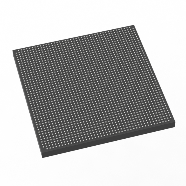
Overview of 5SGSED8N3F45C4N – Stratix V GS FPGA, 695,000 logic elements, 1932‑FBGA
The 5SGSED8N3F45C4N is a Stratix® V GS field programmable gate array (FPGA) in a high‑density 1932‑FBGA package. It combines the Stratix V family architecture with abundant DSP resources and integrated transceiver capability to address transceiver‑based, DSP‑centric applications.
This commercial‑grade device provides large on‑chip logic and memory capacity, extensive I/O, and low‑voltage core operation for designs that require dense logic, significant embedded memory, and high I/O connectivity within the Stratix V product family.
Key Features
- Core & architecture Based on the Stratix V family architecture with the redesigned adaptive logic module (ALM) and a comprehensive fabric clocking network.
- Logic capacity 695,000 logic elements for implementing complex digital designs.
- Embedded memory Approximately 51.2 Mbits of on‑chip RAM, supported by 20 Kbit (M20K) embedded memory blocks.
- DSP resources Variable‑precision DSP blocks in the Stratix V GS family supporting up to 3,926 18×18 or 1,963 27×27 multipliers for high‑throughput signal processing.
- Transceivers Stratix V GS devices include integrated transceivers with 14.1‑Gbps data rate capability for backplane and optical interfaces.
- I/O and package 840 user I/Os in a surface‑mount 1932‑BBGA (1932‑FBGA, FC (45x45)) package for high I/O density and board‑level integration.
- Power and thermal Core voltage supply range of 820 mV to 880 mV and commercial operating temperature range of 0°C to 85°C.
- System integration Family features include fractional PLLs, multi‑track routing, and an Embedded HardCopy Block for hardening IP such as PCIe Gen3/Gen2/Gen1.
- Compliance RoHS‑compliant.
Typical Applications
- Transceiver‑based DSP systems High‑precision digital signal processing where abundant DSP multipliers and on‑chip memory accelerate FIR, FFT, and other algorithms.
- Optical and backplane interfaces Systems requiring integrated high‑speed transceivers for 14.1‑Gbps class backplane or optical links.
- High‑performance compute and networking Packet processing, traffic management, and compute‑intensive tasks that leverage large logic capacity and high I/O counts.
- PCI Express‑enabled subsystems Designs that implement PCIe interfaces using hardened Embedded HardCopy Blocks for lower integration risk.
Unique Advantages
- High logic density: 695,000 logic elements enable complex functions and large‑scale designs without external CPLD/FPGA partitioning.
- Substantial on‑chip memory: Approximately 51.2 Mbits of embedded RAM reduce external memory dependency for buffering and state storage.
- DSP‑oriented resources: Large counts of variable‑precision DSP multipliers accelerate signal processing and algorithmic workloads.
- Dense I/O in a compact package: 840 I/Os in a 1932‑FBGA footprint support high‑pin‑count interfaces while minimizing PCB area.
- Low‑voltage core operation: 820–880 mV supply range helps optimize power for core logic in power‑sensitive designs.
- Stratix V family integration: Family features such as fractional PLLs, multi‑track routing, and Embedded HardCopy Block support simplify system‑level implementation and IP hardening paths.
Why Choose 5SGSED8N3F45C4N?
The 5SGSED8N3F45C4N positions itself as a high‑capacity Stratix V GS FPGA suitable for applications that require dense logic, large embedded memory, extensive DSP resources, and plentiful I/O. Its family‑level features and Embedded HardCopy Block support provide design scalability and options for IP hardening.
This device is well suited for engineers and systems that need a commercial‑grade Stratix V GS device with significant on‑chip resources and integrated transceiver capability, offering a clear path from prototype to production within the Stratix V ecosystem.
Request a quote or submit an RFQ to our sales team for pricing and availability of 5SGSED8N3F45C4N.


Date Founded: 1968
Headquarters: Santa Clara, California, USA
Employees: 130,000+
Revenue: $54.23 Billion
Certifications and Memberships: ISO9001:2015, ISO14001:2015, ISO17025:2017, ISO27001:2022, ISO45001:2018, ISO50001:2018


