
5SGSMD3E1H29C1G
| Part Description |
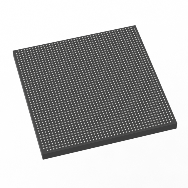
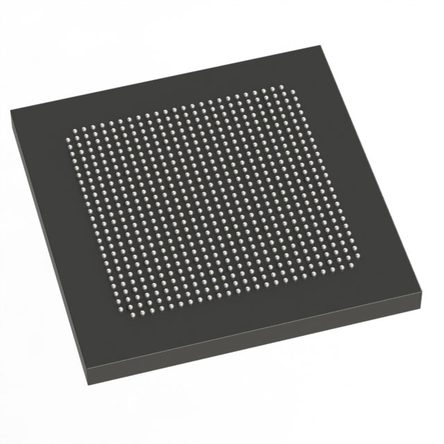
Stratix® V GS Field Programmable Gate Array (FPGA) IC 360 13312000 236000 780-BBGA, FCBGA |
|---|---|
| Quantity | 315 Available (as of June 15, 2026) |

| Product Category | Field Programmable Gate Array (FPGA) |
|---|---|
| Manufacturer | Intel |
| Manufacturing Status | Active |
| Manufacturer Standard Lead Time | 26 Weeks |
| Datasheet |
Specifications & Environmental
| Device Package | 780-HBGA (33x33) | Grade | Commercial | Operating Temperature | 0°C – 85°C | ||
|---|---|---|---|---|---|---|---|
| Package / Case | 780-BBGA, FCBGA | Number of I/O | 360 | Voltage | 870 mV - 930 mV | ||
| Mounting Method | Surface Mount | RoHS Compliance | RoHS Compliant | REACH Compliance | REACH Unaffected | ||
| Moisture Sensitivity Level | 3 (168 Hours) | Number of LABs/CLBs | 89000 | Number of Logic Elements/Cells | 236000 | ||
| Number of Gates | N/A | ECCN | N/A | HTS Code | N/A | ||
| Qualification | N/A | Total RAM Bits | 13312000 |
Overview of 5SGSMD3E1H29C1G – Stratix® V GS FPGA, 360 I/O, ~13.3 Mbit RAM, 236,000 logic elements, 780-BBGA (FCBGA)
The 5SGSMD3E1H29C1G is a Stratix® V GS Field Programmable Gate Array (FPGA) in a 780-ball BGA (FCBGA) package designed for commercial applications. It provides a high logic density and substantial on-chip memory for designs that require extensive programmable logic, embedded RAM, and a large I/O count.
With 236,000 logic element cells, approximately 13.3 Mbits of embedded memory and 360 I/O pins, this device targets complex digital designs where integration, I/O capacity, and low-voltage core operation are key considerations.
Key Features
- Core Logic 236,000 logic element cells to implement complex combinational and sequential logic at high density.
- Embedded Memory Approximately 13.3 Mbits of on-chip RAM to support large buffering, state storage, and data-path requirements.
- I/O Capacity 360 configurable I/O pins for broad system connectivity and flexible interface routing.
- Package Options 780-ball BGA (FCBGA) package; supplier device package listed as 780-HBGA (33×33) for compact, high-density board integration.
- Low-Voltage Core Core supply range specified at 870 mV to 930 mV to support targeted system power architectures.
- Commercial Temperature Grade Rated for commercial operation from 0 °C to 85 °C.
- Standards Compliance RoHS compliant for environmental and manufacturing compatibility.
Typical Applications
- High-density digital logic — Implement complex, large-scale programmable logic functions that require hundreds of thousands of logic elements and significant embedded RAM.
- System prototyping and integration — Consolidate multiple functions into a single FPGA with large I/O capacity for rapid development and system-level validation.
- Custom compute and data-path acceleration — Use the device’s large logic and memory resources to create application-specific acceleration and data buffering solutions.
Unique Advantages
- High logic density: 236,000 logic element cells provide the headroom to implement large, complex designs without immediate partitioning across devices.
- Significant embedded memory: Approximately 13.3 Mbits of on-chip RAM reduces reliance on external memory for many buffering and storage needs, simplifying board design.
- Generous I/O count: 360 I/Os enable extensive peripheral and interface connectivity from a single package.
- Compact package footprint: 780-ball FCBGA (780-HBGA, 33×33) offers a space-efficient solution for high-pin-count FPGA integration.
- Low-voltage core operation: 0.87–0.93 V supply range aligns with modern power-optimized system architectures.
- Commercial-grade reliability: Specified 0 °C to 85 °C operating range for standard commercial deployments.
Why Choose 5SGSMD3E1H29C1G?
The 5SGSMD3E1H29C1G delivers a balanced combination of high logic capacity, substantial embedded RAM, and broad I/O in a compact 780-ball BGA package. It is suited to engineers and system designers who need to integrate complex programmable logic and memory-intensive functions while maintaining a streamlined board footprint and low-voltage core operation.
Choose this Stratix® V GS device when your design calls for high integration, ample on-chip memory, and extensive connectivity within a commercial temperature-grade FPGA platform backed by documented electrical and switching characteristics for the Stratix V family.
Request a quote or submit a purchase inquiry for part number 5SGSMD3E1H29C1G to receive pricing, availability, and ordering information.


Date Founded: 1968
Headquarters: Santa Clara, California, USA
Employees: 130,000+
Revenue: $54.23 Billion
Certifications and Memberships: ISO9001:2015, ISO14001:2015, ISO17025:2017, ISO27001:2022, ISO45001:2018, ISO50001:2018


