
5SGSMD3E1H29C1N
| Part Description |
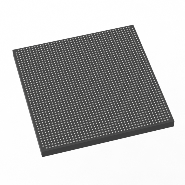
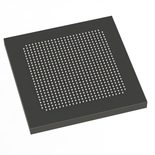
Stratix® V GS Field Programmable Gate Array (FPGA) IC 360 13312000 236000 780-BBGA, FCBGA |
|---|---|
| Quantity | 1,536 Available (as of June 15, 2026) |

| Product Category | Field Programmable Gate Array (FPGA) |
|---|---|
| Manufacturer | Intel |
| Manufacturing Status | Obsolete |
| Manufacturer Standard Lead Time | Contact Us |
| Datasheet |
Specifications & Environmental
| Device Package | 780-HBGA (33x33) | Grade | Commercial | Operating Temperature | 0°C – 85°C | ||
|---|---|---|---|---|---|---|---|
| Package / Case | 780-BBGA, FCBGA | Number of I/O | 360 | Voltage | 870 mV - 930 mV | ||
| Mounting Method | Surface Mount | RoHS Compliance | RoHS Compliant | REACH Compliance | REACH Unknown | ||
| Moisture Sensitivity Level | 3 (168 Hours) | Number of LABs/CLBs | 89000 | Number of Logic Elements/Cells | 236000 | ||
| Number of Gates | N/A | ECCN | 3A001A2C | HTS Code | 8542.39.0001 | ||
| Qualification | N/A | Total RAM Bits | 13312000 |
Overview of 5SGSMD3E1H29C1N – Stratix® V GS FPGA, 236,000 logic elements, 360 I/Os
The 5SGSMD3E1H29C1N is a Stratix V GS field-programmable gate array (FPGA) optimized for DSP-centric, transceiver-based designs. It combines a high logic element count with abundant embedded memory and support for high-speed transceivers, making it suitable for wireline, broadcast, military, and high-performance computing applications.
Built on Stratix V architecture, this commercial-grade, surface-mount FCBGA device provides a path from prototyping to production using Intel's HardCopy V ASIC flow and is intended for designs that require substantial on-chip memory, DSP capability, and flexible I/O.
Key Features
- Core Architecture Stratix V GS family architecture with adaptive logic modules (ALMs) and high-density logic fabric; this device provides 236,000 logic elements for complex logic implementation.
- Embedded Memory Approximately 13.312 Mbits of on-chip RAM (13,312,000 bits) implemented in M20K memory blocks for buffering, packet processing, and algorithm state storage.
- DSP Resources GS-class variable-precision DSP blocks (family-level feature) designed for high-precision digital signal processing workloads.
- Transceiver Capability Integrated transceivers at GS device data rates (family-level capability of up to 14.1 Gbps), enabling high-bandwidth serial interfaces for backplane and optical links.
- Clocking and PLLs Fractional phase-locked loops (PLLs) and a comprehensive fabric clocking network to support complex timing and multi-rate designs (family-level feature).
- Package and I/O 780-ball BGA FCBGA package (supplier package: 780-HBGA, 33×33) with 360 user I/Os for dense board-level integration and high pin-count designs.
- Power and Operating Conditions Core supply voltage range 0.870 V to 0.930 V; commercial operating temperature range 0 °C to 85 °C; surface-mount mounting type.
- Production Path Stratix V family supports a low-risk, low-cost migration path to HardCopy V ASICs for higher-volume production (family-level capability).
- Compliance RoHS compliant for lead-free assembly and regulatory alignment.
Typical Applications
- High‑Performance DSP Systems — Implements compute-intensive algorithms using the device’s variable-precision DSP blocks and large on-chip memory for low-latency processing.
- Wireline and Packet Processing — Provides the logic density, memory, and transceiver capability needed for backplane and line-rate packet processing functions.
- Broadcast and Video Infrastructure — Supports high-bandwidth serial interfaces and on-chip buffering for video transport, transcoding, and format conversion tasks.
- Defense and Aerospace (Commercial‑Temp) — Enables signal processing and high-speed I/O for military communications and test equipment within a commercial temperature range.
- High‑Performance Computing Front Ends — Serves as a configurable front-end for acceleration, data aggregation, and pre-processing in HPC systems.
Unique Advantages
- High logic capacity: 236,000 logic elements enable complex custom logic implementations and large control/data-path designs without partitioning across multiple devices.
- Significant embedded memory: Approximately 13.312 Mbits of on-chip RAM reduce external memory dependencies and improve system latency.
- Transceiver-ready: GS family transceiver capability at 14.1 Gbps (family-level) simplifies integration of high-speed serial links for optical and backplane applications.
- Production scalability: Compatibility with the HardCopy V ASIC path supports migration from FPGA prototyping to production ASICs for volume manufacturing.
- Board-level integration: 360 I/Os in a 780-ball FCBGA package provide dense connectivity for high-pin-count interfaces while maintaining a surface-mount footprint.
- Commercial-grade operation: Designed for 0 °C to 85 °C operation and RoHS compliance for broad deployment in commercial systems.
Why Choose 5SGSMD3E1H29C1N?
The 5SGSMD3E1H29C1N delivers a balanced combination of logic density, embedded memory, DSP capability, and high-speed I/O in a commercial‑grade Stratix V GS FPGA. Its feature set is targeted at designers building transceiver-driven, DSP-intensive systems that require on-chip memory and flexible interfacing.
For teams planning from prototype to production, this Stratix V GS device supports established migration options and family-level hard IP blocks, enabling a predictable development path and design reuse across high-bandwidth and compute-focused product lines.
Request a quote or submit an inquiry to receive pricing and availability for part number 5SGSMD3E1H29C1N.


Date Founded: 1968
Headquarters: Santa Clara, California, USA
Employees: 130,000+
Revenue: $54.23 Billion
Certifications and Memberships: ISO9001:2015, ISO14001:2015, ISO17025:2017, ISO27001:2022, ISO45001:2018, ISO50001:2018


