
5SGSMD3H3F35I4G
| Part Description |
Stratix® V GS Field Programmable Gate Array (FPGA) IC 432 13312000 236000 1152-BBGA, FCBGA |
|---|---|
| Quantity | 331 Available (as of June 15, 2026) |

| Product Category | Field Programmable Gate Array (FPGA) |
|---|---|
| Manufacturer | Intel |
| Manufacturing Status | Active |
| Manufacturer Standard Lead Time | 26 Weeks |
| Datasheet |
Specifications & Environmental
| Device Package | 1152-FBGA (35x35) | Grade | Industrial | Operating Temperature | -40°C – 100°C | ||
|---|---|---|---|---|---|---|---|
| Package / Case | 1152-BBGA, FCBGA | Number of I/O | 432 | Voltage | 820 mV - 880 mV | ||
| Mounting Method | Surface Mount | RoHS Compliance | RoHS Compliant | REACH Compliance | REACH Unaffected | ||
| Moisture Sensitivity Level | 3 (168 Hours) | Number of LABs/CLBs | 89000 | Number of Logic Elements/Cells | 236000 | ||
| Number of Gates | N/A | ECCN | N/A | HTS Code | N/A | ||
| Qualification | N/A | Total RAM Bits | 13312000 |
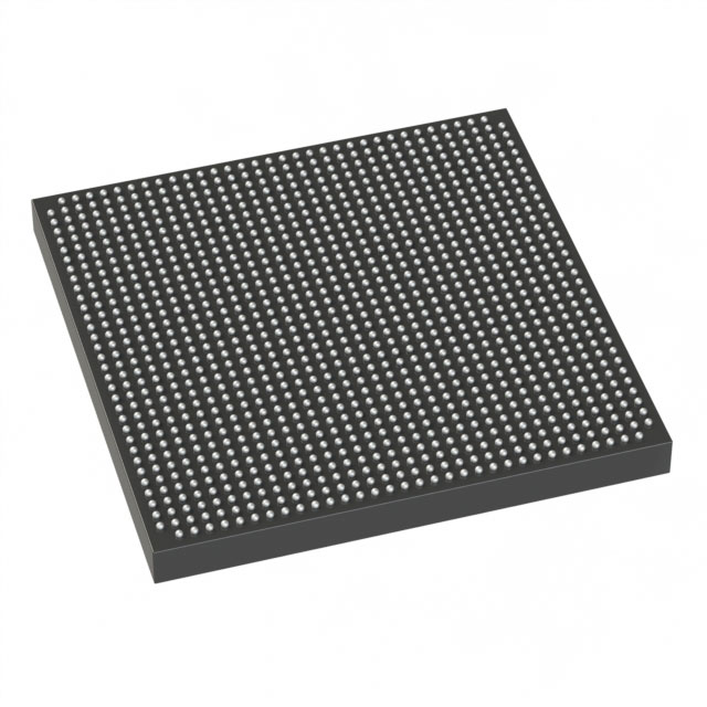
Overview of 5SGSMD3H3F35I4G – Stratix® V GS FPGA, 236,000 logic elements, 432 I/O, 1152‑BBGA
The 5SGSMD3H3F35I4G is an Intel Stratix® V GS Field Programmable Gate Array (FPGA) offered in an industrial temperature grade. This high-density, surface-mount device provides large programmable logic capacity, substantial on-chip memory, and a high I/O count in a 1152‑FBGA (35×35) package.
Designed for applications that require significant embedded memory, many I/O pins, and compact high‑pin‑count packaging, the device operates across an industrial temperature range and at a low core voltage, enabling integration into demanding systems that require reliable, documented FPGA silicon.
Key Features
- Logic Capacity — Provides 236,000 logic elements for complex programmable logic and large-scale design implementation.
- Embedded Memory — Approximately 13.3 Mbits of on‑chip RAM (13,312,000 total RAM bits) to support large buffers, FIFOs, and memory-intensive logic functions.
- I/O Density — 432 user I/O pins to support multiple high‑pin interfaces and board-level integration requirements.
- Package and Mounting — Available in a 1152‑BBGA FCBGA form factor; supplier device package listed as 1152‑FBGA (35×35). Surface‑mount mounting type for modern PCB assembly.
- Power Envelope — Core supply range of 820 mV to 880 mV for low‑voltage core operation.
- Industrial Temperature Grade — Rated for operation from −40°C to 100°C to meet extended-range thermal requirements.
- Regulatory — RoHS compliant.
- Documentation — Part of the Stratix V family covered by Intel/Altera device datasheet material describing electrical and switching characteristics, I/O timing, and package/density information.
Typical Applications
- High‑density data processing systems — Use the device’s 236,000 logic elements and large embedded memory to implement complex DSP and custom compute pipelines.
- Multi‑interface bridging and protocol aggregation — 432 I/O pins accommodate numerous parallel or serial interfaces for aggregation, protocol conversion, and board‑level bridging.
- Prototyping and system integration — The FCBGA package and extensive logic resources enable prototyping of large FPGA designs and integration into production systems requiring industrial temperature operation.
Unique Advantages
- High logic density: 236,000 logic elements allow large and complex designs to be implemented on a single device, reducing system BOM complexity.
- Substantial on‑chip memory: Approximately 13.3 Mbits of embedded RAM supports large buffering and local storage, minimizing external memory dependence.
- High I/O count: 432 user I/Os provide flexibility for interfacing to multiple peripherals, mezzanine modules, or high‑pin connectors without external expanders.
- Industrial thermal range: Rated from −40°C to 100°C for reliable operation in extended‑temperature applications.
- Compact high‑pin package: 1152‑FBGA (35×35) offers a dense, surface‑mount solution for space‑constrained boards while preserving routing capacity.
- Documented platform: Part of the Stratix V family with accessible electrical and switching characteristic documentation for design validation and power/timing planning.
Why Choose 5SGSMD3H3F35I4G?
The 5SGSMD3H3F35I4G delivers a balance of high programmable logic capacity, sizable embedded memory, and a high I/O count in a compact 1152‑FBGA package. Its industrial temperature rating and low core voltage range make it suitable for systems that need robust, low‑voltage FPGA silicon with documented electrical and switching characteristics.
This device is well suited to engineering teams building large, memory‑heavy logic designs or integrating numerous interfaces on a single FPGA. Backed by Stratix V family documentation, it provides the technical detail required for power, timing, and I/O planning during development and production.
Request a quote or submit an inquiry to obtain pricing, availability, and ordering information for the 5SGSMD3H3F35I4G.


Date Founded: 1968
Headquarters: Santa Clara, California, USA
Employees: 130,000+
Revenue: $54.23 Billion
Certifications and Memberships: ISO9001:2015, ISO14001:2015, ISO17025:2017, ISO27001:2022, ISO45001:2018, ISO50001:2018


