
5SGSMD4E1H29C1N
| Part Description |
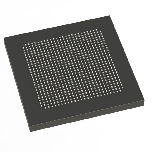
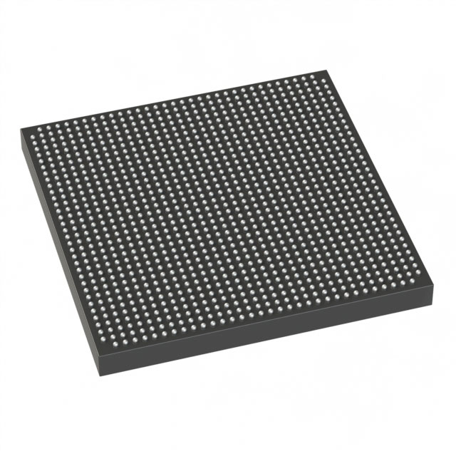
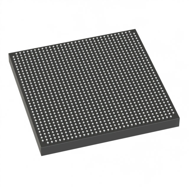
Stratix® V GS Field Programmable Gate Array (FPGA) IC 360 19456000 360000 780-BBGA, FCBGA |
|---|---|
| Quantity | 1,415 Available (as of October 8, 2026) |
| Product Category | Field Programmable Gate Array (FPGA) |
|---|---|
| Manufacturer | Intel |
| Manufacturing Status | Obsolete |
| Manufacturer Standard Lead Time | Contact Us |
| Datasheet |
Specifications & Environmental
| Device Package | 780-HBGA (33x33) | Grade | Commercial | Operating Temperature | 0°C – 85°C | ||
|---|---|---|---|---|---|---|---|
| Package / Case | 780-BBGA, FCBGA | Number of I/O | 360 | Voltage | 870 mV - 930 mV | ||
| Mounting Method | Surface Mount | RoHS Compliance | RoHS Compliant | REACH Compliance | REACH Unknown | ||
| Moisture Sensitivity Level | 3 (168 Hours) | Number of LABs/CLBs | 135840 | Number of Logic Elements/Cells | 360000 | ||
| Number of Gates | N/A | ECCN | 3A001A2C | HTS Code | 8542.39.0001 | ||
| Qualification | N/A | Total RAM Bits | 19456000 |
Overview of 5SGSMD4E1H29C1N – Stratix® V GS Field Programmable Gate Array (FPGA)
The 5SGSMD4E1H29C1N is a Stratix V GS variant FPGA offered in a 780-ball BGA package for surface-mount applications. Built on a 28‑nm architecture, this device targets transceiver‑based, DSP‑centric designs that require high logic density, substantial on‑chip memory, and extensive I/O.
With 360,000 logic elements, integrated high‑speed transceiver capability, and approximately 19.456 Mbits of embedded memory, this FPGA is suited for applications in wireline communications, broadcast, and high‑performance computing where programmable DSP and I/O integration are priorities.
Key Features
- Core & process 28‑nm process architecture with a core supply range of 0.870 V to 0.930 V, optimized for the Stratix V family.
- Logic capacity 360,000 logic elements to support complex FPGA designs and high‑density logic implementation.
- Embedded memory Approximately 19.456 Mbits of on‑chip RAM implemented as M20K memory blocks for buffering and large data structures.
- DSP resources Abundant variable‑precision DSP support—family documentation cites support for up to 3,926 18×18 or 1,963 27×27 multipliers—enabling high‑performance signal processing.
- I/O and transceivers 360 I/O pins and integrated transceiver capability consistent with Stratix V GS devices; transceivers support 14.1‑Gbps data rates for backplane and optical interfaces.
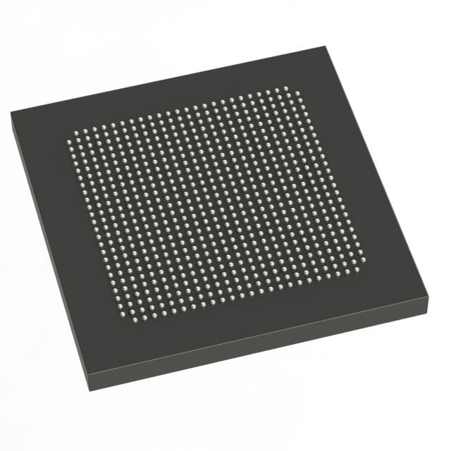
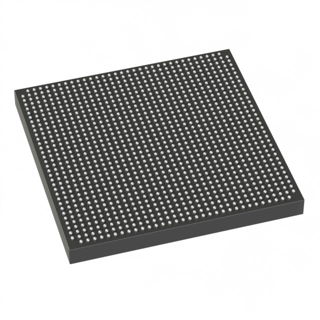
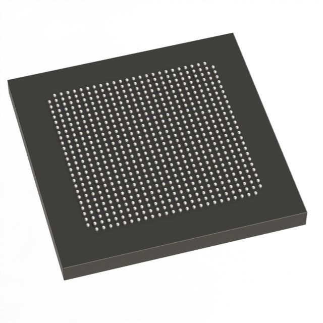
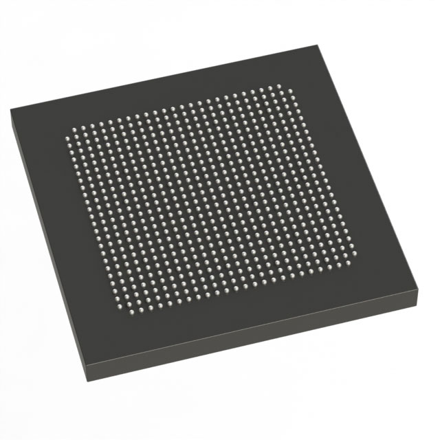
- Package & mounting 780‑ball BGA (FCBGA), supplier package referenced as 780‑HBGA (33×33), designed for surface‑mount assembly.
- Operating conditions Commercial grade with an operating temperature range of 0 °C to 85 °C.
- Standards & compliance RoHS‑compliant component suitable for environmentally compliant designs.
Typical Applications
- Wireline communications: Used for packet processing, traffic management, and backplane interface logic where dense programmable logic and integrated transceivers are required.
- Broadcast and signal processing: Deployed in DSP‑centric systems for video and audio processing that leverage the device’s variable‑precision DSP resources.
- High‑performance computing: Useful for accelerator and data‑path functions that need large logic capacity and fast on‑chip memory.
- Optical transport and networking: Integrates transceiver capability and high I/O count for 40G/100G optical interface and transport applications.
Unique Advantages
- High logic density: 360,000 logic elements provide the headroom to implement large, complex designs on a single device, reducing board‑level component count.
- Integrated DSP capability: Variable‑precision DSP blocks with a high multiplier count accelerate signal processing tasks without external ASICs.
- On‑chip memory capacity: Approximately 19.456 Mbits of embedded RAM supports large buffers and data structures, improving system throughput and latency.
- Transceiver support: GS‑family transceiver capability (14.1‑Gbps class) enables integration of high‑speed serial links for backplane and optical interfaces.
- Commercial packaging for surface mount: 780‑ball BGA (33×33) package simplifies board design for production assemblies while providing high I/O density.
- Regulatory compliance: RoHS compliance supports environmentally responsible product development.
Why Choose 5SGSMD4E1H29C1N?
The 5SGSMD4E1H29C1N combines large logic capacity, substantial embedded memory, and DSP‑oriented resources in a Stratix V GS device tailored for transceiver and DSP‑centric applications. Its 360,000 logic elements and family‑level transceiver capabilities make it a practical choice for designers targeting high‑performance communications, broadcast, and compute acceleration tasks.
For teams requiring scalable performance and a programmable platform with strong on‑chip integration, this Stratix V GS FPGA provides a robust foundation, backed by the Stratix V device family architecture and ecosystem support documented for the series.
Request a quote or submit an inquiry to purchase the 5SGSMD4E1H29C1N and discuss lead time, pricing, and volume availability with our sales team.





















Date Founded: 1968
Headquarters: Santa Clara, California, USA
Employees: 130,000+
Revenue: $54.23 Billion
Certifications and Memberships: ISO9001:2015, ISO14001:2015, ISO17025:2017, ISO27001:2022, ISO45001:2018, ISO50001:2018


