
5SGSMD4H2F35C1N
| Part Description |
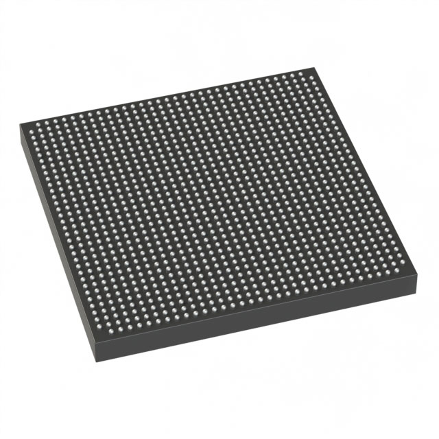
Stratix® V GS Field Programmable Gate Array (FPGA) IC 432 19456000 360000 1152-BBGA, FCBGA |
|---|---|
| Quantity | 97 Available (as of June 14, 2026) |

| Product Category | Field Programmable Gate Array (FPGA) |
|---|---|
| Manufacturer | Intel |
| Manufacturing Status | Obsolete |
| Manufacturer Standard Lead Time | Contact Us |
| Datasheet |
Specifications & Environmental
| Device Package | 1152-FBGA (35x35) | Grade | Commercial | Operating Temperature | 0°C – 85°C | ||
|---|---|---|---|---|---|---|---|
| Package / Case | 1152-BBGA, FCBGA | Number of I/O | 432 | Voltage | 870 mV - 930 mV | ||
| Mounting Method | Surface Mount | RoHS Compliance | RoHS Compliant | REACH Compliance | REACH Unknown | ||
| Moisture Sensitivity Level | 3 (168 Hours) | Number of LABs/CLBs | 135840 | Number of Logic Elements/Cells | 360000 | ||
| Number of Gates | N/A | ECCN | 3A001A2C | HTS Code | 8542.39.0001 | ||
| Qualification | N/A | Total RAM Bits | 19456000 |
Overview of 5SGSMD4H2F35C1N – Stratix® V GS FPGA, 360,000 logic elements, 1152-BBGA
The 5SGSMD4H2F35C1N is a Stratix® V GS field programmable gate array (FPGA) IC optimized for DSP-centric and transceiver-based designs. Built on the Stratix V family architecture, it pairs a high logic element count with abundant embedded memory and integrated transceiver capabilities to address bandwidth- and compute-intensive applications.
This commercial-grade device combines a high-density fabric with series-level hard IP and system building blocks, providing designers with a platform for high-performance digital signal processing, packet processing, and high-bandwidth communications.
Key Features
- Core architecture (28 nm) — Stratix V family architecture with enhanced adaptive logic modules (ALMs) and a comprehensive fabric clocking network.
- Logic density — 360,000 logic elements for implementing large, complex user logic and control functions.
- Embedded memory — Approximately 19.456 Mbits of on-chip RAM (Total RAM Bits: 19,456,000) using 20-Kbit (M20K) memory blocks for buffering and data storage.
- Variable-precision DSP resources — GS variant DSP architecture supports up to 3,926 18×18 or 1,963 27×27 multipliers for high-performance signal processing.
- Integrated transceivers — GS devices include transceivers with 14.1-Gbps data-rate capability for backplane and optical interface applications.
- I/O and package — 432 user I/Os in a surface-mount 1152-BBGA (1152-FBGA, 35×35) package providing high-density board-level connectivity.
- Power — Core voltage supply range of 870 mV to 930 mV to match system power-architecture requirements.
- Operating range and compliance — Commercial-grade device with an operating temperature of 0 °C to 85 °C and RoHS compliance.
- Hard IP and system blocks — Family-level Embedded HardCopy Block and hard IP support (for PCIe Gen3/Gen2/Gen1 instantiation) plus fractional PLLs and multi-track routing fabric.
Typical Applications
- High-performance DSP systems — Leverage the large DSP multiplier count and abundant on-chip RAM for real-time signal processing and algorithm acceleration.
- Optical and backplane communications — Integrated transceivers with 14.1-Gbps capability suit 40G/100G applications and high-speed optical interfaces.
- Packet processing and networking — High logic density and extensive I/O enable complex packet engines, traffic management, and protocol processing.
- Broadcast and compute-intensive applications — Large embedded memory and DSP resources support video processing, encoding, and other compute-heavy workflows.
Unique Advantages
- High integration density: 360,000 logic elements and approximately 19.456 Mbits of embedded RAM reduce the need for external logic and memory, simplifying board design.
- DSP-optimized architecture: Large count of variable-precision multipliers enables efficient implementation of filter, transform, and other signal-processing blocks.
- High-speed connectivity: Integrated transceivers capable of 14.1 Gbps provide native support for demanding serial interfaces and high-bandwidth links.
- Robust system building blocks: On-chip PLLs, M20K memory blocks, and adaptive logic modules support deterministic timing and modular design reuse.
- Compact, high-density package: 1152-BBGA (35×35) surface-mount package accommodates many I/Os in a space-efficient footprint for board-level integration.
- Power-flexible core: 870 mV to 930 mV core supply range enables compatibility with a variety of system power architectures.
Why Choose 5SGSMD4H2F35C1N?
The 5SGSMD4H2F35C1N positions itself as a capable Stratix V GS device for engineers who need a balance of high logic capacity, substantial on-chip memory, powerful DSP resources, and integrated high-speed transceivers. Its combination of architecture-level building blocks and hard IP support makes it suitable for demanding communications, DSP, and networking designs that require both compute and bandwidth.
Designed for commercial applications, this FPGA offers scalability and a clear upgrade path within the Stratix V family, enabling development and production workflows that leverage family-level tools and resources.
Request a quote or submit a purchase inquiry to receive pricing and availability information for 5SGSMD4H2F35C1N.


Date Founded: 1968
Headquarters: Santa Clara, California, USA
Employees: 130,000+
Revenue: $54.23 Billion
Certifications and Memberships: ISO9001:2015, ISO14001:2015, ISO17025:2017, ISO27001:2022, ISO45001:2018, ISO50001:2018


