
5SGSMD8K3F40C2LN
| Part Description |
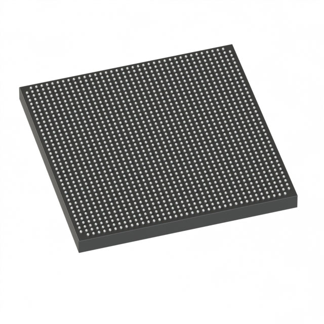
Stratix® V GS Field Programmable Gate Array (FPGA) IC 696 51200000 695000 1517-BBGA, FCBGA |
|---|---|
| Quantity | 593 Available (as of October 8, 2026) |
| Product Category | Field Programmable Gate Array (FPGA) |
|---|---|
| Manufacturer | Intel |
| Manufacturing Status | Obsolete |
| Manufacturer Standard Lead Time | Contact Us |
| Datasheet |
Specifications & Environmental
| Device Package | 1517-FBGA (40x40) | Grade | Commercial | Operating Temperature | 0°C – 85°C | ||
|---|---|---|---|---|---|---|---|
| Package / Case | 1517-BBGA, FCBGA | Number of I/O | 696 | Voltage | 820 mV - 880 mV | ||
| Mounting Method | Surface Mount | RoHS Compliance | RoHS Compliant | REACH Compliance | REACH Unknown | ||
| Moisture Sensitivity Level | 3 (168 Hours) | Number of LABs/CLBs | 262400 | Number of Logic Elements/Cells | 695000 | ||
| Number of Gates | N/A | ECCN | 3A001A2C | HTS Code | 8542.39.0001 | ||
| Qualification | N/A | Total RAM Bits | 51200000 |
Overview of 5SGSMD8K3F40C2LN – Stratix® V GS Field Programmable Gate Array (FPGA) IC 696 I/Os, ~51.2 Mbits RAM, 695,000 Logic Elements
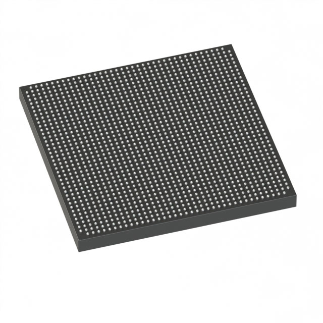
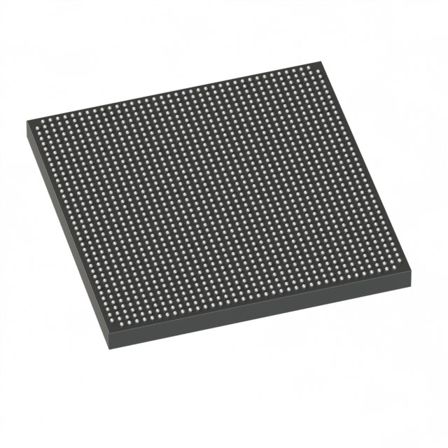
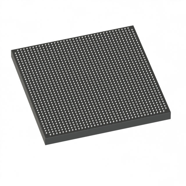
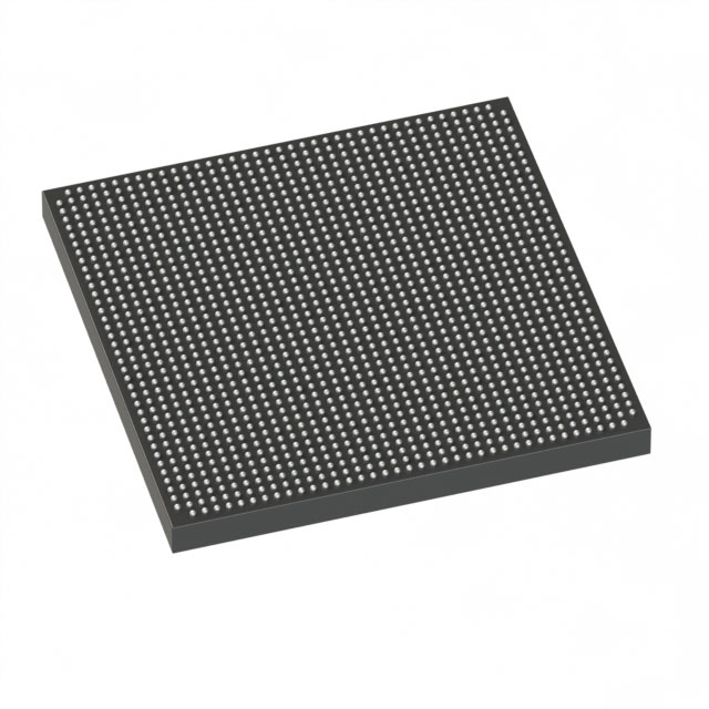
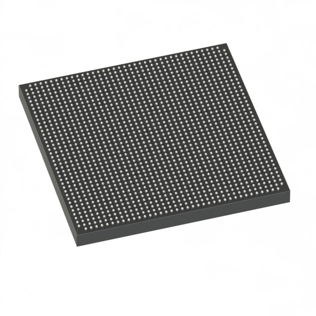
The 5SGSMD8K3F40C2LN is a Stratix V GS field programmable gate array (FPGA) offered in a 1517‑ball FCBGA package. It delivers very high logic density and a large on‑chip memory footprint, combined with extensive I/O capability for complex, board‑level integration.
Designed for commercial‑grade applications, this device is optimized for designs that require hundreds of thousands of logic elements, substantial embedded RAM, and a large number of external interfaces while operating within a 0 °C to 85 °C temperature range and a core supply of 820 mV to 880 mV.
Key Features
- Core Logic Capacity — 695,000 logic elements provide a very high-density fabric for complex digital functions and large-scale integration.
- Logic Fabric Resources — 262,400 logic array blocks (CLBs/LABs equivalent) to structure and organize designs at scale.
- Embedded Memory — Approximately 51.2 Mbits of total on‑chip RAM to support buffering, lookup tables, and on‑die data storage.
- I/O Richness — 696 user I/Os for extensive peripheral, interface, and board interconnect options.
- Power and Supply — Core voltage specified from 820 mV to 880 mV for regulated, predictable power planning.
- Package & Mounting — 1517‑BBGA (FCBGA) package, supplier device package 1517‑FBGA (40×40); surface‑mount device suitable for high‑density PCB assembly.
- Commercial Grade Temperature — Rated for 0 °C to 85 °C operating temperature for standard commercial environments.
- Regulatory Compliance — RoHS compliant.
Typical Applications
- High‑density digital signal processing — Large logic capacity and substantial embedded RAM support complex DSP pipelines and algorithm implementation.
- Network and communications equipment — Hundreds of I/Os and high logic resources enable protocol processing, packet handling, and interface bridging.
- Imaging and video processing — Ample logic and on‑chip memory for frame buffering, parallel processing, and pixel‑level operations.
- Compute acceleration and custom hardware — Large fabric and memory footprint suitable for hardware acceleration tasks and bespoke compute blocks.
Unique Advantages
- Very high logic density: 695,000 logic elements allow consolidation of large designs onto a single device, reducing board‑level complexity.
- Substantial embedded memory: Approximately 51.2 Mbits of RAM supports on‑chip data storage to minimize external memory dependence and latency.
- Extensive I/O count: 696 I/Os provide flexibility for interfacing with multiple peripherals, mezzanine cards, or high‑pin count connectors.
- Commercial temperature support: Rated 0 °C to 85 °C for mainstream environments and applications.
- Surface‑mount FCBGA package: 1517‑ball FCBGA (40×40) supports high‑density PCB designs and automated assembly processes.
- RoHS compliant: Meets common environmental sourcing requirements for commercial products.
Why Choose 5SGSMD8K3F40C2LN?
The 5SGSMD8K3F40C2LN is positioned for commercial designs that need a combination of very high logic capacity, significant embedded memory, and broad I/O capability in a single FPGA package. Its specifications make it suitable for consolidating complex functions, implementing large custom accelerators, and supporting multi‑interface systems while operating within standard commercial temperature and supply ranges.
For engineering teams targeting scalability and integration on compact boards, this Stratix V GS device offers the measurable resources and package attributes to reduce external components, simplify routing, and support demanding FPGA designs with predictable electrical and thermal constraints.
Request a quote or submit a procurement inquiry to learn about availability, volume pricing, and lead times for the 5SGSMD8K3F40C2LN.





















Date Founded: 1968
Headquarters: Santa Clara, California, USA
Employees: 130,000+
Revenue: $54.23 Billion
Certifications and Memberships: ISO9001:2015, ISO14001:2015, ISO17025:2017, ISO27001:2022, ISO45001:2018, ISO50001:2018


