
5SGSMD8N3F45C3G
| Part Description |
Stratix® V GS Field Programmable Gate Array (FPGA) IC 840 51200000 695000 1932-BBGA, FCBGA |
|---|---|
| Quantity | 724 Available (as of June 15, 2026) |

| Product Category | Field Programmable Gate Array (FPGA) |
|---|---|
| Manufacturer | Intel |
| Manufacturing Status | Active |
| Manufacturer Standard Lead Time | 26 Weeks |
| Datasheet |
Specifications & Environmental
| Device Package | 1932-FBGA, FC (45x45) | Grade | Commercial | Operating Temperature | 0°C – 85°C | ||
|---|---|---|---|---|---|---|---|
| Package / Case | 1932-BBGA, FCBGA | Number of I/O | 840 | Voltage | 820 mV - 880 mV | ||
| Mounting Method | Surface Mount | RoHS Compliance | RoHS Compliant | REACH Compliance | REACH Unaffected | ||
| Moisture Sensitivity Level | 3 (168 Hours) | Number of LABs/CLBs | 262400 | Number of Logic Elements/Cells | 695000 | ||
| Number of Gates | N/A | ECCN | N/A | HTS Code | N/A | ||
| Qualification | N/A | Total RAM Bits | 51200000 |
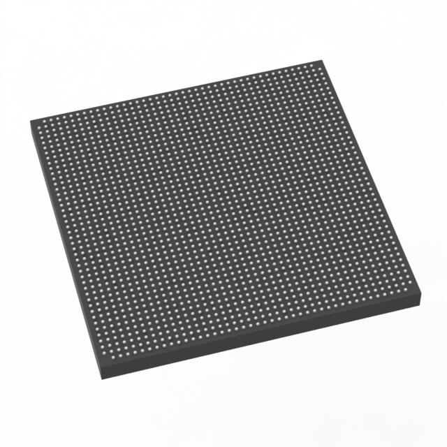
Overview of 5SGSMD8N3F45C3G – Stratix V GS FPGA, 695,000 logic elements, 51.2 Mbit RAM, 840 I/Os, 1932-BBGA
The 5SGSMD8N3F45C3G is a Stratix® V GS Field Programmable Gate Array (FPGA) from Intel, supplied in a 1932-ball FCBGA package. It delivers very high logic density and on-chip memory capacity, along with a large I/O count, intended for commercial-grade programmable logic applications.
With 695,000 logic elements, approximately 51.2 Mbits of embedded memory and 840 I/Os, this device is suited for designs that require extensive logic, significant embedded RAM and broad external connectivity while operating within a commercial temperature range.
Key Features
- Logic Capacity 695,000 logic elements to implement large, complex FPGA designs and high-density logic functions.
- Embedded Memory Approximately 51.2 Mbits of on-chip RAM for buffer, lookup table and state-storage requirements without external memory.
- I/O Density 840 programmable I/Os to support wide parallel interfaces, multiple peripherals and high-pin-count system designs.
- Power/Core Supply Specified core voltage supply range of 820 mV to 880 mV to match system power delivery and design constraints.
- Package and Mounting 1932-BBGA (FCBGA) package; supplier device package listed as 1932-FBGA, FC (45×45). Surface-mount mounting type for standard PCB assembly.
- Operating Temperature Commercial-grade operation from 0 °C to 85 °C for typical commercial-environment deployments.
- Regulatory RoHS compliant.
Typical Applications
- High-density compute and acceleration Use the device's large logic capacity and embedded RAM to implement custom accelerators and data-path processing within commercial equipment.
- Networking and packet processing High I/O count and on-chip memory enable wide parallel interfaces and buffering for communication and switching platforms.
- Signal processing Leverage extensive logic resources and embedded memory for DSP pipelines, filters and real-time data manipulation in commercial systems.
- Prototyping and system integration A high-density FPGA option for integrating multiple system functions into a single programmable device during development and integration phases.
Unique Advantages
- Substantial logic resources: 695,000 logic elements provide headroom for complex designs and multi-function integration, reducing the need for discrete ASICs or multiple FPGAs.
- Large on-chip memory: Approximately 51.2 Mbits of embedded RAM supports buffering and state retention for high-throughput data flows without external DRAM.
- Extensive I/O capability: 840 I/Os enable broad peripheral connectivity and parallel data interfaces, simplifying board-level routing for high-pin-count applications.
- Commercial-grade profile: Specified for 0 °C to 85 °C operation and RoHS compliance, aligning with standard commercial electronic product requirements.
- Compact FCBGA package: The 1932-ball FCBGA (45×45) package provides a high-density form factor suitable for space-constrained PCBs using standard surface-mount assembly.
Why Choose 5SGSMD8N3F45C3G?
This Stratix V GS FPGA balances very high logic density, substantial embedded memory and broad I/O capability in a single commercial-grade FCBGA package. It is positioned for engineers and system designers who need to consolidate complex digital functions, large buffering needs and multiple interfaces into a single programmable device while operating within standard commercial temperature and power envelopes.
Choosing this part supports scalable designs that require significant on-chip resources and flexible I/O mapping, backed by Intel’s Stratix V device family documentation and electrical characteristic specifications.
Request a quote or submit an inquiry to get pricing and availability for the 5SGSMD8N3F45C3G and to discuss lead times or volume requirements.


Date Founded: 1968
Headquarters: Santa Clara, California, USA
Employees: 130,000+
Revenue: $54.23 Billion
Certifications and Memberships: ISO9001:2015, ISO14001:2015, ISO17025:2017, ISO27001:2022, ISO45001:2018, ISO50001:2018


