
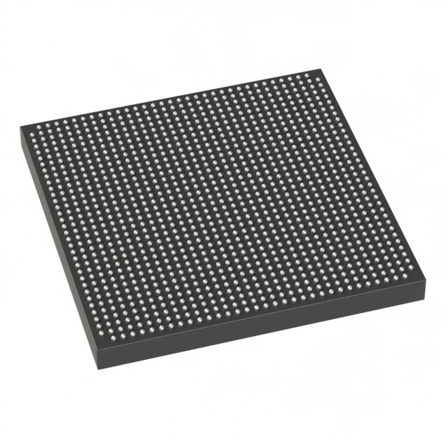
5SGXEA3K1F35I2G
| Part Description |
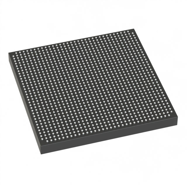
Stratix® V GX Field Programmable Gate Array (FPGA) IC 432 19456000 340000 1152-BBGA, FCBGA |
|---|---|
| Quantity | 826 Available (as of October 8, 2026) |
| Product Category | Field Programmable Gate Array (FPGA) |
|---|---|
| Manufacturer | Intel |
| Manufacturing Status | Active |
| Manufacturer Standard Lead Time | 26 Weeks |
| Datasheet |
Specifications & Environmental
| Device Package | 1152-FBGA (35x35) | Grade | Industrial | Operating Temperature | -40°C – 100°C | ||
|---|---|---|---|---|---|---|---|
| Package / Case | 1152-BBGA, FCBGA | Number of I/O | 432 | Voltage | 870 mV - 930 mV | ||
| Mounting Method | Surface Mount | RoHS Compliance | RoHS Compliant | REACH Compliance | REACH Unaffected | ||
| Moisture Sensitivity Level | 3 (168 Hours) | Number of LABs/CLBs | 128300 | Number of Logic Elements/Cells | 340000 | ||
| Number of Gates | N/A | ECCN | N/A | HTS Code | N/A | ||
| Qualification | N/A | Total RAM Bits | 19456000 |
Overview of 5SGXEA3K1F35I2G – Stratix® V GX Field Programmable Gate Array (FPGA) IC
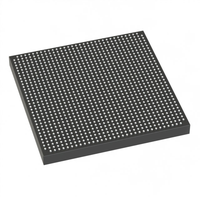
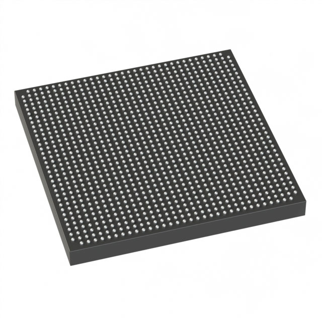
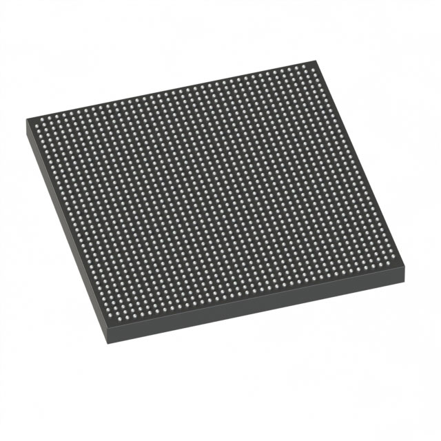
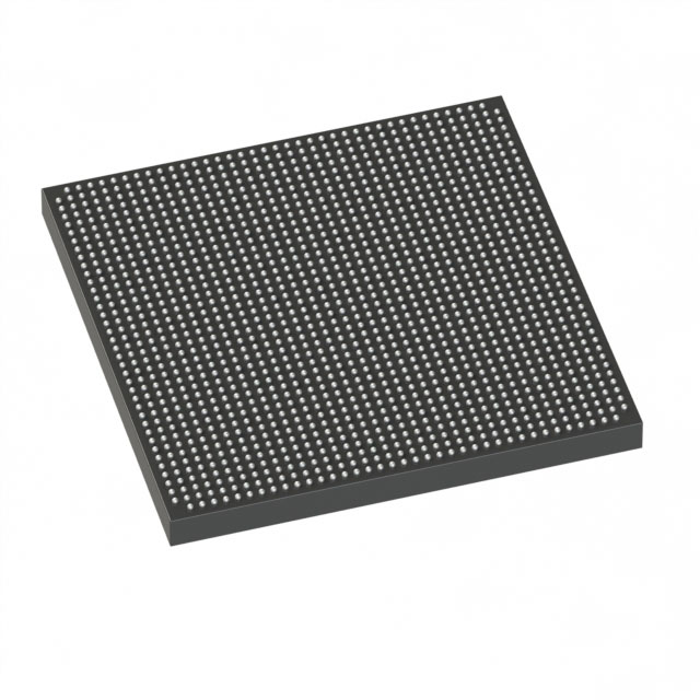
The 5SGXEA3K1F35I2G is a Stratix V GX field-programmable gate array in an industrial-grade FCBGA package. It combines high logic density, substantial embedded memory, and a large I/O complement for demanding system designs that require programmable hardware resources.
With approximately 340,000 logic elements, roughly 19.46 Mbits of embedded memory, and 432 I/O pins, this device targets high-density implementations where integration, thermal margin, and configurable silicon are primary concerns. The device supports industrial temperature operation from –40°C to 100°C and operates from a core supply of 870 mV to 930 mV.
Key Features
- Core Logic Approximately 340,000 logic elements organized with a reported 128,300 LABs/CLBs for complex, high-density programmable logic implementations.
- On‑Chip Memory Approximately 19.46 Mbits of embedded RAM for buffering, packet memory, and intermediate storage within programmable logic.
- I/O Capability 432 I/O pins to support high-pin-count interfaces and dense external connectivity in a single device.
- Transceiver Speed Grades As a Stratix V GX device family member, the series includes GX transceiver speed grades documented in the datasheet (for example, GX channel listings such as 14.1 Gbps and 12.5 Gbps across supported grades).
- Power and Voltage Core supply voltage specified between 870 mV and 930 mV, enabling designs targeting the device's published operating window.
- Package and Mounting 1152-ball BGA FCBGA (supplier package listed as 1152-FBGA, 35×35) in a surface-mount form factor for compact board integration.
- Industrial Temperature Grade Rated for operation from –40°C to 100°C, suitable for industrial-environment deployments.
- RoHS Compliant Device is RoHS compliant, meeting standard environmental requirements for lead-free assembly.
Typical Applications
- High-density programmable logic Implement large-scale custom logic functions and hardware accelerators using the device's ~340,000 logic elements and abundant on-chip RAM.
- Systems requiring extensive I/O Designs needing a high pin-count interface can leverage the device's 432 I/Os for parallel and serial connectivity.
- Industrial equipment Use in industrial systems that require operation across –40°C to 100°C and benefit from a resilient, high-integration FPGA.
- High-speed serial links Take advantage of the Stratix V GX family transceiver speed grades documented in the device series to support high-bandwidth serial channels.
Unique Advantages
- High logic density: ~340,000 logic elements provide headroom for complex state machines, datapath logic, and custom processors.
- Substantial embedded memory: Approximately 19.46 Mbits of on-chip RAM reduces reliance on external memory for many buffering and storage tasks.
- Extensive I/O resources: 432 I/Os minimize the need for external expanders in high-connectivity designs.
- Industrial temperature operation: Specified –40°C to 100°C rating suits deployments with wide thermal ranges.
- Compact surface-mount FCBGA: 1152-ball package (35×35) enables dense PCB placement while supporting a high I/O count.
- Low-voltage core operation: 870–930 mV core supply range supports designs that align power delivery and thermal budgets to the device's published operating window.
Why Choose 5SGXEA3K1F35I2G?
The 5SGXEA3K1F35I2G brings together significant programmable logic capacity, large embedded memory, and a high I/O count in an industrial-temperature FCBGA package. Its electrical and transceiver characteristics, as documented for the Stratix V GX family, make it suitable for complex, high-throughput designs where integration and thermal robustness are required.
This device is well suited for engineering teams designing scalable, high-density FPGA-based systems that need reliable operation across extended temperature ranges, compact board integration, and the configurable resources provided by the Stratix V GX series.
Request a quote or submit a pricing inquiry for the 5SGXEA3K1F35I2G through your preferred procurement or quotation channel to evaluate fit for your next design.





















Date Founded: 1968
Headquarters: Santa Clara, California, USA
Employees: 130,000+
Revenue: $54.23 Billion
Certifications and Memberships: ISO9001:2015, ISO14001:2015, ISO17025:2017, ISO27001:2022, ISO45001:2018, ISO50001:2018


