
5SGXEA4H1F35C1G
| Part Description |
Stratix® V GX Field Programmable Gate Array (FPGA) IC 552 37888000 420000 1152-BBGA, FCBGA |
|---|---|
| Quantity | 1,065 Available (as of June 14, 2026) |
| Product Category | Field Programmable Gate Array (FPGA) |
|---|---|
| Manufacturer | Intel |
| Manufacturing Status | Active |
| Manufacturer Standard Lead Time | 26 Weeks |
| Datasheet |
Specifications & Environmental
| Device Package | 1152-FBGA (35x35) | Grade | Commercial | Operating Temperature | 0°C – 85°C | ||
|---|---|---|---|---|---|---|---|
| Package / Case | 1152-BBGA, FCBGA | Number of I/O | 552 | Voltage | 870 mV - 930 mV | ||
| Mounting Method | Surface Mount | RoHS Compliance | RoHS Compliant | REACH Compliance | REACH Unaffected | ||
| Moisture Sensitivity Level | 3 (168 Hours) | Number of LABs/CLBs | 158500 | Number of Logic Elements/Cells | 420000 | ||
| Number of Gates | N/A | ECCN | N/A | HTS Code | N/A | ||
| Qualification | N/A | Total RAM Bits | 37888000 |
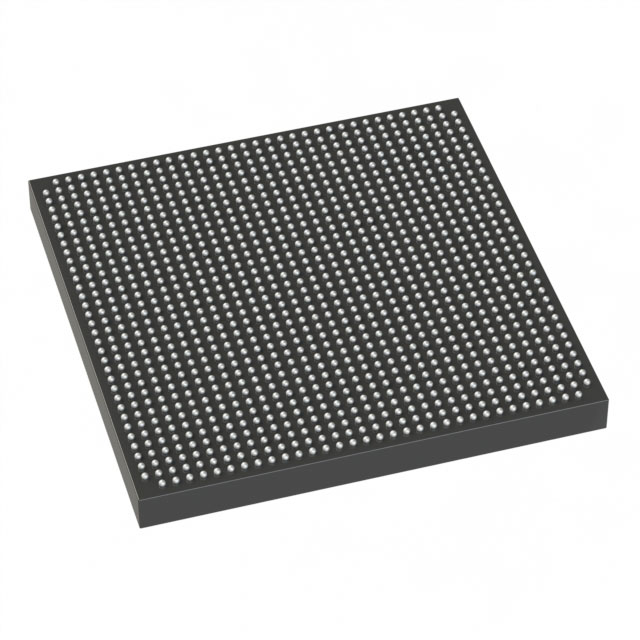
Overview of 5SGXEA4H1F35C1G – Stratix V GX FPGA, 420,000 logic elements, 1152‑BBGA
The 5SGXEA4H1F35C1G is a Stratix® V GX field programmable gate array designed for high-density, high‑I/O system implementations. It integrates 420,000 logic elements and approximately 38 Mbits of on‑chip RAM to address complex digital signal processing, networking, and compute-acceleration tasks.
This device is supplied in a 1152‑FBGA (35×35) package for surface‑mount assembly and offers 552 device I/Os. It is a commercial‑grade part specified for operation from 0 °C to 85 °C and a core supply range of 870 mV to 930 mV.
Key Features
- Core Logic 420,000 logic elements for high-density logic implementation and complex finite-state machines or datapaths.
- Embedded Memory Approximately 38 Mbits of on‑chip RAM to support FIFOs, buffers, and on-chip data storage.
- I/O Capacity 552 device I/Os to enable large, multi‑lane interfaces, parallel sensors, and broad connectivity options.
- Package & Mounting 1152‑FBGA (35×35) package case (1152‑BBGA, FCBGA) in a surface‑mount form factor for compact board integration.
- Power Core supply specified from 870 mV to 930 mV for predictable power planning and supply rail design.
- Operating Range Commercial grade operation from 0 °C to 85 °C suitable for controlled‑environment electronics.
- Regulatory RoHS compliant.
Typical Applications
- High‑Performance Networking Large logic capacity and extensive I/O make the device suitable for packet processing, protocol bridging, and multi‑lane interface aggregation.
- Data Center Acceleration Dense logic and on‑chip memory enable custom compute kernels and hardware offload functions.
- Signal Processing On‑chip RAM and abundant logic support real‑time DSP, filtering, and multichannel data acquisition tasks.
- Prototyping and System Integration High I/O count and a compact BGA package facilitate integration into evaluation platforms and prototype systems requiring many external interfaces.
Unique Advantages
- High logic density: 420,000 logic elements provide the headroom needed for complex designs without immediate migration to larger devices.
- Substantial embedded memory: Approximately 38 Mbits of RAM reduces dependency on external memory for many buffering and state‑holding tasks.
- Extensive I/O availability: 552 I/Os simplify board-level routing and allow direct connections to multiple high‑speed peripherals or parallel interfaces.
- Compact BGA footprint: 1152‑FBGA (35×35) package enables a dense, manufacturable solution for space‑constrained PCBs.
- Commercial temperature and RoHS compliance: Device grading and environmental compliance support mainstream electronic product development and deployment.
Why Choose 5SGXEA4H1F35C1G?
The 5SGXEA4H1F35C1G delivers a balanced combination of high logic capacity, significant on‑chip memory, and a large I/O count in a compact BGA package, making it well suited for demanding data‑path and processing applications in commercial products. Its defined operating voltage window and commercial temperature rating simplify system power design and thermal planning.
Designed as part of the Stratix V GX family, this device fits design flows that require large FPGA resources and broad connectivity while remaining within commercial environmental constraints. It offers a scalable option for teams developing networking, signal processing, and compute‑acceleration solutions that need substantial on‑chip integration and predictable electrical characteristics.
Request a quote or submit an inquiry to discuss availability, lead times, and how the 5SGXEA4H1F35C1G can meet your project requirements.


Date Founded: 1968
Headquarters: Santa Clara, California, USA
Employees: 130,000+
Revenue: $54.23 Billion
Certifications and Memberships: ISO9001:2015, ISO14001:2015, ISO17025:2017, ISO27001:2022, ISO45001:2018, ISO50001:2018


