
5SGXEA3K3F40I3LN
| Part Description |
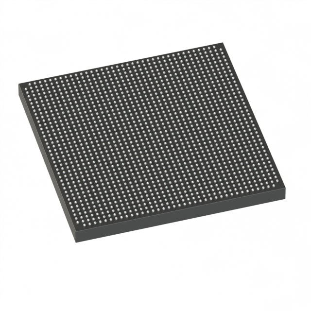
Stratix® V GX Field Programmable Gate Array (FPGA) IC 696 19456000 340000 1517-BBGA, FCBGA |
|---|---|
| Quantity | 1,929 Available (as of June 8, 2026) |

| Product Category | Field Programmable Gate Array (FPGA) |
|---|---|
| Manufacturer | Intel |
| Manufacturing Status | Obsolete |
| Manufacturer Standard Lead Time | Contact Us |
| Datasheet |
Specifications & Environmental
| Device Package | 1517-FBGA (40x40) | Grade | Industrial | Operating Temperature | -40°C – 100°C | ||
|---|---|---|---|---|---|---|---|
| Package / Case | 1517-BBGA, FCBGA | Number of I/O | 696 | Voltage | 820 mV - 880 mV | ||
| Mounting Method | Surface Mount | RoHS Compliance | RoHS Compliant | REACH Compliance | REACH Unknown | ||
| Moisture Sensitivity Level | 3 (168 Hours) | Number of LABs/CLBs | 128300 | Number of Logic Elements/Cells | 340000 | ||
| Number of Gates | N/A | ECCN | 3A001A2C | HTS Code | 8542.39.0001 | ||
| Qualification | N/A | Total RAM Bits | 19456000 |
Overview of 5SGXEA3K3F40I3LN – Stratix® V GX Field Programmable Gate Array (FPGA), 340,000 logic elements, 696 I/Os
The 5SGXEA3K3F40I3LN is a Stratix V GX Field Programmable Gate Array (FPGA) IC from Intel, designed to provide very large logic capacity and extensive I/O in a single surface-mount package. It delivers a combination of high logic element count, substantial on-chip memory, and an industrial operating temperature range for demanding embedded and system-level applications.
As a member of the Stratix V GX family (see the Stratix V device datasheet for series-level electrical and switching characteristics), this device targets designs that require large programmable logic resources, high I/O counts, and industrial-grade thermal performance.
Key Features
- Core Logic Approximately 340,000 logic elements and 128,300 LABs, providing extensive programmable fabric for complex logic, DSP, and glue-logic implementations.
- Embedded Memory Approximately 19.456 Mbits of on-chip RAM to support large buffers, FIFOs, and state storage without external memory for many design tasks.
- I/O Capacity 696 user I/Os to support dense connectivity, multi-channel interfaces, and broad peripheral integration.
- Power and Supply Core voltage supply range from 820 mV to 880 mV to match system power rails and power budgeting requirements.
- Package and Mounting 1517-BBGA FCBGA (supplier package: 1517-FBGA, 40×40), surface-mount package optimized for high pin count applications and compact board footprints.
- Thermal and Grade Industrial grade device with an operating temperature range of –40 °C to 100 °C for extended-temperature applications.
- Compliance RoHS compliant for alignment with environmental and manufacturing standards.
Typical Applications
- High-density digital processing Large logic capacity and on-chip RAM enable complex algorithm implementation and parallel processing on a single device.
- Multi-channel I/O aggregation 696 I/Os support systems that require broad interface consolidation and signal routing in a compact form factor.
- Industrial control and automation Industrial temperature rating and robust packaging make the device suitable for control, monitoring, and embedded computing in harsh environments.
- System integration and protocol bridging Extensive logic and memory resources allow implementation of protocol conversion, bridging, and custom peripheral controllers without extensive external components.
Unique Advantages
- Very large programmable fabric: Approximately 340,000 logic elements enable integration of multiple functions into a single FPGA, reducing board-level complexity.
- Significant on-chip memory: About 19.456 Mbits of embedded RAM reduces dependence on external memory for buffering and state retention.
- High I/O count: 696 I/Os provide flexibility for complex system interconnects and high channel-density designs.
- Industrial temperature operation: Rated from –40 °C to 100 °C to maintain functionality across a wide range of deployment conditions.
- Compact high-pin-count package: 1517-BBGA FCBGA (1517-FBGA, 40×40) combines a small footprint with a large number of available signals for dense system designs.
- RoHS compliant: Meets lead-free manufacturing requirements for many production environments.
Why Choose 5SGXEA3K3F40I3LN?
The 5SGXEA3K3F40I3LN positions itself as a high-capacity, I/O-rich Stratix V GX FPGA suitable for designs that demand substantial programmable logic, significant embedded RAM, and broad connectivity in an industrial-temperature, surface-mount package. Its combination of approximately 340,000 logic elements, roughly 19.456 Mbits of on-chip RAM, and 696 I/Os enables consolidation of functions and reduces external component count for system-level simplification.
This device is well suited to engineering teams building dense digital systems, multi-interface controllers, or industrial embedded platforms that require scalable, reliable programmable logic with the long-term support and documentation provided for the Stratix V family.
Request a quote or submit an inquiry to obtain pricing, availability, and lead-time information for the 5SGXEA3K3F40I3LN.


Date Founded: 1968
Headquarters: Santa Clara, California, USA
Employees: 130,000+
Revenue: $54.23 Billion
Certifications and Memberships: ISO9001:2015, ISO14001:2015, ISO17025:2017, ISO27001:2022, ISO45001:2018, ISO50001:2018


