
5SGXEA4H2F35C2N
| Part Description |
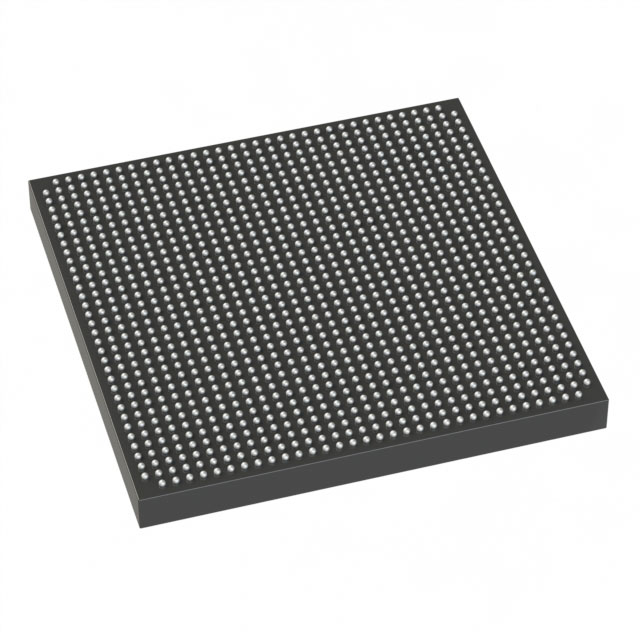
Stratix® V GX Field Programmable Gate Array (FPGA) IC 552 37888000 420000 1152-BBGA, FCBGA |
|---|---|
| Quantity | 352 Available (as of October 7, 2026) |
| Product Category | Field Programmable Gate Array (FPGA) |
|---|---|
| Manufacturer | Intel |
| Manufacturing Status | Obsolete |
| Manufacturer Standard Lead Time | Contact Us |
| Datasheet |
Specifications & Environmental
| Device Package | 1152-FBGA (35x35) | Grade | Commercial | Operating Temperature | 0°C – 85°C | ||
|---|---|---|---|---|---|---|---|
| Package / Case | 1152-BBGA, FCBGA | Number of I/O | 552 | Voltage | 870 mV - 930 mV | ||
| Mounting Method | Surface Mount | RoHS Compliance | RoHS Compliant | REACH Compliance | REACH Unknown | ||
| Moisture Sensitivity Level | 3 (168 Hours) | Number of LABs/CLBs | 158500 | Number of Logic Elements/Cells | 420000 | ||
| Number of Gates | N/A | ECCN | 3A001A2C | HTS Code | 8542.39.0001 | ||
| Qualification | N/A | Total RAM Bits | 37888000 |
Overview of 5SGXEA4H2F35C2N – Stratix® V GX FPGA – 420,000 Logic Elements, 552 I/Os
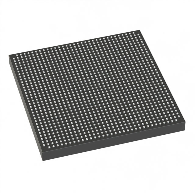
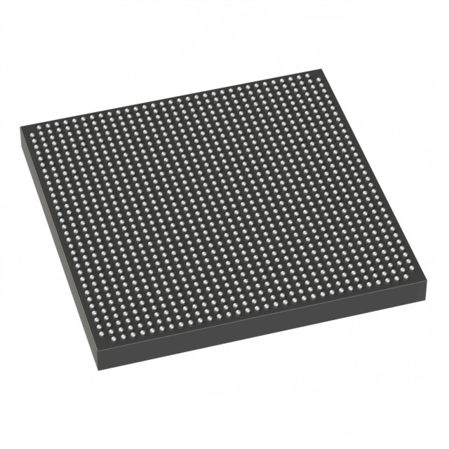
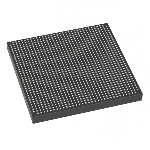
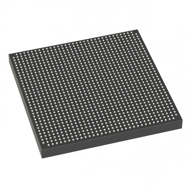
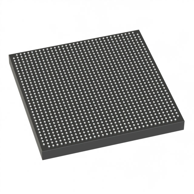
The 5SGXEA4H2F35C2N is a Stratix® V GX Field Programmable Gate Array (FPGA) in a 1152‑BBGA (FCBGA) package. It provides a high density of programmable logic, on‑chip memory, and a large I/O count suitable for complex digital designs.
Engineered for commercial‑grade applications, this device combines 420,000 logic elements, approximately 38 Mbits of embedded RAM, and 552 I/Os to support designs that require significant logic capacity and extensive interfacing. Voltage and thermal operating ranges are optimized for standard commercial system environments.
Key Features
- Core Logic Density 420,000 logic elements and 158,500 LABs/CLBs provide substantial programmable fabric for large FPGA designs.
- Embedded Memory Total on‑chip RAM of 37,888,000 bits (approximately 37.9 Mbits) supports buffering, FIFOs, and on‑chip data storage.
- I/O Capacity & Package 552 I/Os in a 1152‑BBGA FCBGA (35 × 35 mm) package enable high pin‑count connectivity for complex system interfaces.
- Power Supply Core voltage range specified at 870 mV to 930 mV to match system power delivery requirements.
- Mounting & Grade Surface mount package offered in a commercial temperature grade with an operating range of 0 °C to 85 °C.
- Compliance RoHS‑compliant manufacturing and materials.
- Family-Level Transceiver Options As a Stratix V GX device, the family includes defined transceiver speed grades in the device datasheet; refer to family documentation for available transceiver speed‑grade selections and characteristics.
Unique Advantages
- High logic capacity: 420,000 logic elements enable integration of complex algorithms and large custom IP blocks on a single device.
- Substantial embedded memory: Approximately 38 Mbits of on‑chip RAM reduces reliance on external memory for many buffering and storage needs.
- Extensive I/O availability: 552 I/Os support multiple high‑pin interfaces and dense board connectivity without additional multiplexing hardware.
- Compact high‑density package: 1152‑BBGA FCBGA (35 × 35 mm) balances board space and routing density for compact, high‑performance systems.
- Commercial operating range: 0 °C to 85 °C provides predictable performance across standard commercial deployments.
- Industry compliance: RoHS status reduces regulatory and supply‑chain risk for standard commercial products.
Why Choose 5SGXEA4H2F35C2N?
This Stratix V GX FPGA delivers a combination of large logic capacity, significant on‑chip memory, and a high I/O count in a compact FCBGA package, making it well suited for complex commercial designs that require dense programmable logic and extensive interfacing. The device’s defined voltage range and commercial temperature grade align with typical commercial system power and environmental conditions.
As part of the Stratix V family, the device benefits from documented device and transceiver characteristics in the Stratix V device datasheet, providing the technical detail necessary for system integration and speed‑grade selection. Its RoHS compliance and high integration help reduce BOM complexity while supporting scalable FPGA designs.
If you would like pricing, availability, or a formal quote for 5SGXEA4H2F35C2N, request a quote or submit an inquiry to obtain current lead‑time and procurement details.





















Date Founded: 1968
Headquarters: Santa Clara, California, USA
Employees: 130,000+
Revenue: $54.23 Billion
Certifications and Memberships: ISO9001:2015, ISO14001:2015, ISO17025:2017, ISO27001:2022, ISO45001:2018, ISO50001:2018


