
5SGXEA4K2F40C1G
| Part Description |
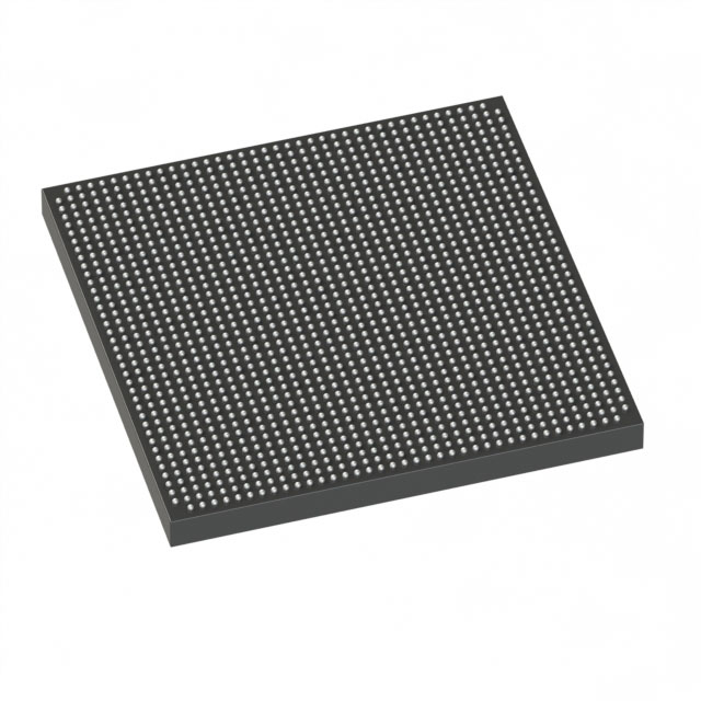
Stratix® V GX Field Programmable Gate Array (FPGA) IC 696 37888000 420000 1517-BBGA, FCBGA |
|---|---|
| Quantity | 202 Available (as of June 14, 2026) |

| Product Category | Field Programmable Gate Array (FPGA) |
|---|---|
| Manufacturer | Intel |
| Manufacturing Status | Active |
| Manufacturer Standard Lead Time | 26 Weeks |
| Datasheet |
Specifications & Environmental
| Device Package | 1517-FBGA (40x40) | Grade | Commercial | Operating Temperature | 0°C – 85°C | ||
|---|---|---|---|---|---|---|---|
| Package / Case | 1517-BBGA, FCBGA | Number of I/O | 696 | Voltage | 870 mV - 930 mV | ||
| Mounting Method | Surface Mount | RoHS Compliance | RoHS Compliant | REACH Compliance | REACH Unaffected | ||
| Moisture Sensitivity Level | 3 (168 Hours) | Number of LABs/CLBs | 158500 | Number of Logic Elements/Cells | 420000 | ||
| Number of Gates | N/A | ECCN | N/A | HTS Code | N/A | ||
| Qualification | N/A | Total RAM Bits | 37888000 |
Overview of 5SGXEA4K2F40C1G – Stratix® V GX FPGA, 420,000 logic elements, 696 I/Os
The 5SGXEA4K2F40C1G is a Stratix V GX field programmable gate array (FPGA) in a 1517-ball FCBGA package. It delivers a high logic element count, substantial on‑chip memory, and a large I/O complement for complex, programmable digital designs.
Designed for commercial temperature operation, this device targets dense logic integration and high I/O connectivity where programmable hardware resources and on‑chip memory capacity are required.
Key Features
- High-capacity programmable logic — 420,000 logic elements to implement large-scale digital functions and complex custom architectures.
- Embedded memory — approximately 37.9 Mbits of on‑chip RAM for data buffering, state storage, and embedded memory-intensive functions.
- Extensive I/O — 696 user I/Os to support wide external interfacing, parallel buses, and high pin-count system integrations.
- Core power range — core supply range of 870 mV to 930 mV for defined power rail requirements in board design.
- Commercial temperature grade — rated for 0 °C to 85 °C operation for standard commercial applications.
- Package and mounting — 1517‑BBGA / 1517‑FBGA (40×40) FCBGA, surface-mount package suitable for compact board layouts.
- Standards compliance — RoHS compliant to meet current lead‑free regulatory requirements.
Typical Applications
- High-density digital processing — Implement large combinational and sequential logic functions using the device’s 420,000 logic elements and abundant embedded RAM.
- Signal aggregation and protocol bridging — Support complex I/O topologies and wide parallel interfaces with 696 user I/Os for system interconnect and protocol conversion tasks.
- Compute offload and acceleration — Use on‑chip memory and high logic capacity to accelerate compute kernels and data-path functions within commercial compute appliances.
- Prototype and custom SoC implementation — Leverage the device’s logic density and memory resources for proof‑of‑concept and custom hardware prototypes.
Unique Advantages
- Large logic capacity: 420,000 logic elements provide the headroom required for complex, multi‑module designs without excessive partitioning.
- Significant embedded memory: Approximately 37.9 Mbits of on‑chip RAM reduces dependence on external memory for many buffering and state‑storage needs.
- High I/O count: 696 user I/Os simplify board routing and enable wide interfaces or multiple peripheral connections without external expanders.
- Compact FCBGA packaging: 1517‑FBGA (40×40) surface-mount package balances high pin count and PCB area efficiency for dense system boards.
- Commercial temperature rating: Rated 0 °C to 85 °C for mainstream commercial deployments and standard operating environments.
- Regulatory readiness: RoHS compliance supports lead‑free assembly processes and regulatory conformance in commercial products.
Why Choose 5SGXEA4K2F40C1G?
The 5SGXEA4K2F40C1G positions itself as a high-density, commercial‑grade Stratix V GX FPGA suited to applications that require large programmable logic resources, substantial on‑chip RAM, and a very high I/O count. Its defined core voltage range and FCBGA package make it practical for compact, board‑level implementations where integration and I/O flexibility matter.
This device is appropriate for engineering teams building complex digital processing, interface aggregation, or compute‑acceleration solutions that benefit from a single, high‑capacity programmable device backed by the Stratix V family specifications.
Request a quote or submit an inquiry to discuss availability, pricing, and lead time for the 5SGXEA4K2F40C1G.


Date Founded: 1968
Headquarters: Santa Clara, California, USA
Employees: 130,000+
Revenue: $54.23 Billion
Certifications and Memberships: ISO9001:2015, ISO14001:2015, ISO17025:2017, ISO27001:2022, ISO45001:2018, ISO50001:2018


