
5SGXEA5H1F35C2G
| Part Description |
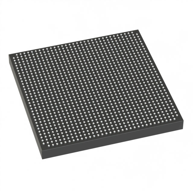
Stratix® V GX Field Programmable Gate Array (FPGA) IC 552 46080000 490000 1152-BBGA, FCBGA |
|---|---|
| Quantity | 1,063 Available (as of June 10, 2026) |
| Product Category | Field Programmable Gate Array (FPGA) |
|---|---|
| Manufacturer | Intel |
| Manufacturing Status | Active |
| Manufacturer Standard Lead Time | 26 Weeks |
| Datasheet |
Specifications & Environmental
| Device Package | 1152-FBGA (35x35) | Grade | Commercial | Operating Temperature | 0°C – 85°C | ||
|---|---|---|---|---|---|---|---|
| Package / Case | 1152-BBGA, FCBGA | Number of I/O | 552 | Voltage | 870 mV - 930 mV | ||
| Mounting Method | Surface Mount | RoHS Compliance | RoHS Compliant | REACH Compliance | REACH Unaffected | ||
| Moisture Sensitivity Level | 3 (168 Hours) | Number of LABs/CLBs | 185000 | Number of Logic Elements/Cells | 490000 | ||
| Number of Gates | N/A | ECCN | N/A | HTS Code | N/A | ||
| Qualification | N/A | Total RAM Bits | 46080000 |
Overview of 5SGXEA5H1F35C2G – Stratix® V GX Field Programmable Gate Array (FPGA) IC 552 46080000 490000 1152-BBGA, FCBGA
The 5SGXEA5H1F35C2G is a Stratix V GX family FPGA offering large on-chip programmable logic and memory capacity in a surface-mount FCBGA package. It provides approximately 490,000 logic elements and around 46.08 Mbits of embedded RAM, combined with a high I/O count for demanding digital designs.
Designed for commercial-temperature systems, this device targets applications that require substantial programmable logic density, extensive I/O connectivity, and low-voltage core operation in a 1152-FBGA (35×35) package.
Key Features
- Logic Capacity Approximately 490,000 logic elements, supporting complex, large-scale programmable designs.
- Logic Block Count Listed with 185,000 logic blocks, enabling partitioning of designs across a high-density fabric.
- Embedded Memory Approximately 46.08 Mbits of on-chip RAM for buffering, state storage, and memory-intensive functions.
- I/O Resources 552 user I/Os to support extensive external interfaces and multi-channel connectivity.
- Power and Voltage Core voltage supply specified from 870 mV to 930 mV for optimized low-voltage operation.
- Package and Mounting 1152-BBGA, FCBGA package (supplier device package: 1152-FBGA, 35×35) in a surface-mount form factor for high-density system integration.
- Operating Temperature Commercial grade operation from 0 °C to 85 °C.
- RoHS Compliance Device is RoHS-compliant for environmental and regulatory adherence.
- Family-level Transceiver Options Stratix V GX devices are offered with transceiver speed grades as documented for the family; refer to device documentation for grade-specific details.
Typical Applications
- High-density digital processing Large programmable fabric and abundant RAM make this device suitable for compute- and pipeline-heavy digital signal processing tasks.
- Multi‑interface systems High I/O count supports boards and systems requiring many external links, parallel interfaces, or multi-channel connectivity.
- Custom hardware acceleration Large logic and memory resources enable hardware acceleration of algorithms and offloading of compute-intensive functions.
Unique Advantages
- Substantial programmable capacity: With approximately 490,000 logic elements, the device supports complex system-on-chip style implementations without immediate need for multiple FPGAs.
- Large embedded memory: Around 46.08 Mbits of on-chip RAM reduces dependence on external memory for many buffering and scratchpad use cases.
- High I/O availability: 552 I/Os allow flexible partitioning of interfaces and minimize external multiplexing or bridging components.
- Compact, manufacturable package: 1152‑FBGA (35×35) surface-mount package balances pin count and PCB routing density for production designs.
- Commercial temperature suitability: Rated for 0 °C to 85 °C operation to match typical commercial deployments and system environments.
- Regulatory alignment: RoHS compliance supports environmentally conscious product development and regulatory requirements.
Why Choose 5SGXEA5H1F35C2G?
This Stratix V GX FPGA delivers a combination of high logic density, significant embedded RAM, and large I/O capacity in a production-friendly FCBGA package. It is positioned for engineers building feature-rich, compute- and I/O-intensive systems at commercial temperatures where on-chip resources reduce BOM complexity and external component count.
Engineers and procurement teams seeking a high-density, RoHS-compliant FPGA with defined voltage and thermal operating ranges will find this part suitable for scaling complex designs while leveraging documented family-level capabilities in the Stratix V GX series.
Request a quote or submit a pricing inquiry for 5SGXEA5H1F35C2G to obtain availability and ordering information for your design needs.


Date Founded: 1968
Headquarters: Santa Clara, California, USA
Employees: 130,000+
Revenue: $54.23 Billion
Certifications and Memberships: ISO9001:2015, ISO14001:2015, ISO17025:2017, ISO27001:2022, ISO45001:2018, ISO50001:2018


