
5SGXEA5H1F35C2L
| Part Description |
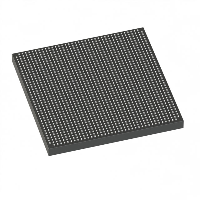
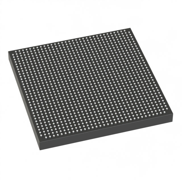
Stratix® V GX Field Programmable Gate Array (FPGA) IC 552 46080000 490000 1152-BBGA, FCBGA |
|---|---|
| Quantity | 1,330 Available (as of June 15, 2026) |

| Product Category | Field Programmable Gate Array (FPGA) |
|---|---|
| Manufacturer | Intel |
| Manufacturing Status | Obsolete |
| Manufacturer Standard Lead Time | Contact Us |
| Datasheet |
Specifications & Environmental
| Device Package | 1152-FBGA (35x35) | Grade | Commercial | Operating Temperature | 0°C – 85°C | ||
|---|---|---|---|---|---|---|---|
| Package / Case | 1152-BBGA, FCBGA | Number of I/O | 552 | Voltage | 820 mV - 880 mV | ||
| Mounting Method | Surface Mount | RoHS Compliance | RoHS Compliant | REACH Compliance | REACH Unknown | ||
| Moisture Sensitivity Level | 3 (168 Hours) | Number of LABs/CLBs | 185000 | Number of Logic Elements/Cells | 490000 | ||
| Number of Gates | N/A | ECCN | 3A001A2C | HTS Code | 8542.39.0001 | ||
| Qualification | N/A | Total RAM Bits | 46080000 |
Overview of 5SGXEA5H1F35C2L – Stratix V GX FPGA, 490,000 logic elements, ~46 Mbits RAM, 552 I/Os, 1152-BBGA
The 5SGXEA5H1F35C2L is a Stratix® V GX Field Programmable Gate Array (FPGA) IC from Intel, delivered in a 1152-ball FCBGA package. It provides large programmable logic capacity, substantial on-chip RAM, and a high I/O count for designs that require dense logic integration and robust I/O routing.
This commercial-grade device is targeted at applications that need significant logic resources and embedded memory while operating within a 0 °C to 85 °C range and a low-voltage core supply of 820 mV to 880 mV.
Key Features
- Logic Capacity — 490,000 logic elements for implementing large-scale digital designs and complex logic functions.
- Embedded Memory — Approximately 46 Mbits of on-chip RAM to support buffering, lookup tables, and state storage without external memory.
- I/O Resources — 552 user I/O pins to accommodate extensive peripheral interfaces, bus connections, and board-level signal routing.
- Package and Mounting — 1152-BBGA (FCBGA) package; supplier device package listed as 1152-FBGA (35×35) and surface-mount mounting for board-level integration.
- Power and Voltage — Core voltage supply range of 820 mV to 880 mV for low-voltage operation.
- Operating Conditions & Grade — Commercial temperature grade with an operating range of 0 °C to 85 °C; RoHS compliant.
Typical Applications
- Complex digital systems — Use the large logic element count to implement extensive custom logic, datapaths, and control functions.
- High-density I/O interfacing — Leverage 552 I/Os for multi-channel I/O, board-level interconnects, and mixed-signal front-end routing.
- Memory-reliant designs — Utilize approximately 46 Mbits of embedded RAM for buffering, packet storage, and algorithmic state retention.
- Prototyping and system integration — Ideal for engineering prototypes and designs that require significant on-chip resources in a single FPGA package.
Unique Advantages
- High programmable density: 490,000 logic elements enable consolidation of complex functions into one device, reducing board-level component count.
- Substantial on-chip memory: Approximately 46 Mbits of embedded RAM minimizes dependence on external memory for many designs, simplifying layout and BOM.
- Extensive I/O capability: 552 I/Os provide flexibility for interfacing to multiple peripherals, buses, and mezzanine connectors.
- Compact BGA footprint: 1152-ball FCBGA package (35×35) supports high-density PCB layouts while maintaining serviceable pin count.
- Low-voltage core operation: Core supply range of 820 mV–880 mV supports power-optimized system architectures.
- Commercial-grade and RoHS compliant: Designed for commercial temperature operation (0 °C–85 °C) and meets RoHS requirements for regulatory compliance.
Why Choose 5SGXEA5H1F35C2L?
The 5SGXEA5H1F35C2L delivers a balance of large programmable logic, ample embedded memory, and abundant I/O in a surface-mount 1152-BBGA package. Its specification set targets designs that require consolidation of complex logic and substantial on-chip buffering while operating at a low-voltage core and within commercial temperature limits.
This device is well suited to engineering teams and system integrators who need a high-capacity FPGA for dense digital designs, extensive I/O requirements, and reduced external memory dependence—providing scalability and integration for medium- to high-complexity projects.
Request a quote or submit a purchase inquiry to obtain pricing, availability, and ordering information for the 5SGXEA5H1F35C2L.


Date Founded: 1968
Headquarters: Santa Clara, California, USA
Employees: 130,000+
Revenue: $54.23 Billion
Certifications and Memberships: ISO9001:2015, ISO14001:2015, ISO17025:2017, ISO27001:2022, ISO45001:2018, ISO50001:2018


