
5SGXEA5H3F35I3LG
| Part Description |
Stratix® V GX Field Programmable Gate Array (FPGA) IC 552 46080000 490000 1152-BBGA, FCBGA |
|---|---|
| Quantity | 1,414 Available (as of June 17, 2026) |

| Product Category | Field Programmable Gate Array (FPGA) |
|---|---|
| Manufacturer | Intel |
| Manufacturing Status | Active |
| Manufacturer Standard Lead Time | 26 Weeks |
| Datasheet |
Specifications & Environmental
| Device Package | 1152-FBGA (35x35) | Grade | Industrial | Operating Temperature | -40°C – 100°C | ||
|---|---|---|---|---|---|---|---|
| Package / Case | 1152-BBGA, FCBGA | Number of I/O | 552 | Voltage | 820 mV - 880 mV | ||
| Mounting Method | Surface Mount | RoHS Compliance | RoHS Compliant | REACH Compliance | REACH Unaffected | ||
| Moisture Sensitivity Level | 3 (168 Hours) | Number of LABs/CLBs | 185000 | Number of Logic Elements/Cells | 490000 | ||
| Number of Gates | N/A | ECCN | N/A | HTS Code | N/A | ||
| Qualification | N/A | Total RAM Bits | 46080000 |
Overview of 5SGXEA5H3F35I3LG – Stratix® V GX FPGA, 490,000 logic elements
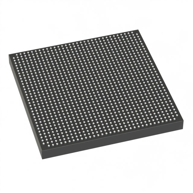
The 5SGXEA5H3F35I3LG is an Intel Stratix V GX field programmable gate array (FPGA) IC offering 490,000 logic elements and approximately 46 Mbits of embedded memory. This device is supplied in a 1152‑BBGA FCBGA package (1152‑FBGA, 35×35) and is designed for surface‑mount PCB assembly.
Targeted for industrial applications, the device provides a broad I/O count (552 I/Os), a low core voltage range (0.820 V to 0.880 V), and an operating temperature range of −40 °C to 100 °C. As a member of the Stratix V GX family, it is positioned for high‑density, high‑integration digital designs that require substantial on‑chip memory and extensive I/O.
Key Features
- High‑density logic — 490,000 logic elements to implement large-scale digital designs and complex FPGA architectures.
- Embedded memory — Approximately 46 Mbits of on‑chip RAM for buffering, packet processing, or local data storage.
- Extensive I/O — 552 user I/Os to support wide parallel interfaces and multi‑lane connectivity.
- Power and core voltage — Core supply voltage range of 0.820 V to 0.880 V to match platform power architectures.
- Industrial temperature grade — Specified operating range from −40 °C to 100 °C for use in industrial environments.
- Package and mounting — 1152‑BBGA (1152‑FBGA, 35×35) FCBGA package; surface‑mount mounting type for standard SMT assembly.
- Compliance — RoHS‑compliant device to meet environmental regulations.
Typical Applications
- Industrial control systems — High logic density and industrial temperature rating enable complex control, real‑time processing, and robust operation in factory or process environments.
- High‑throughput networking and communications — Large logic capacity, substantial embedded memory, and Stratix V GX family transceiver orientation support dense packet processing and multiport interfaces.
- Hardware acceleration and signal processing — On‑chip RAM and extensive logic resources make the device suitable for custom accelerators, DSP pipelines, and data manipulation tasks.
- System integration and prototyping — A broad I/O complement and high logic count simplify integration of complex subsystems and rapid iteration of hardware designs.
Unique Advantages
- High integration density: 490,000 logic elements reduce external component count and consolidate complex functions on a single device.
- Significant on‑chip memory: Approximately 46 Mbits of embedded RAM enable large buffers and localized data storage without external memory in many designs.
- Large I/O footprint: 552 I/Os provide flexibility for parallel interfaces, wide buses, and multiple peripheral connections.
- Industrial reliability: Specified for −40 °C to 100 °C operation to support equipment deployed in harsh or temperature‑variable environments.
- Compact SMT package: 1152‑BBGA FCBGA in a 35×35 format supports dense board layouts while maintaining a repeatable surface‑mount assembly process.
- Regulatory compliance: RoHS compliance assists with regulatory and environmental requirements for modern electronic products.
Why Choose 5SGXEA5H3F35I3LG?
The 5SGXEA5H3F35I3LG positions itself as a high‑density Stratix V GX FPGA for industrial applications that demand large logic capacity, substantial on‑chip memory, and extensive I/O in a compact FCBGA package. Its voltage and temperature specifications make it suitable for designs that require low core‑voltage operation and robust performance across a wide thermal range.
Designers seeking a scalable, high‑integration FPGA element for complex digital systems, networking subsystems, or hardware acceleration can leverage the combination of logic density, embedded RAM, and I/O resources this device provides while maintaining compliance with environmental requirements.
Request a quote or submit a pricing inquiry today to evaluate the 5SGXEA5H3F35I3LG for your next high‑density FPGA design.


Date Founded: 1968
Headquarters: Santa Clara, California, USA
Employees: 130,000+
Revenue: $54.23 Billion
Certifications and Memberships: ISO9001:2015, ISO14001:2015, ISO17025:2017, ISO27001:2022, ISO45001:2018, ISO50001:2018


