
5SGXEA5K3F40I3G
| Part Description |
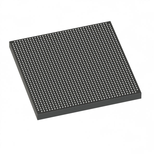
Stratix® V GX Field Programmable Gate Array (FPGA) IC 696 46080000 490000 1517-BBGA, FCBGA |
|---|---|
| Quantity | 143 Available (as of June 10, 2026) |

| Product Category | Field Programmable Gate Array (FPGA) |
|---|---|
| Manufacturer | Intel |
| Manufacturing Status | Active |
| Manufacturer Standard Lead Time | 26 Weeks |
| Datasheet |
Specifications & Environmental
| Device Package | 1517-FBGA (40x40) | Grade | Industrial | Operating Temperature | -40°C – 100°C | ||
|---|---|---|---|---|---|---|---|
| Package / Case | 1517-BBGA, FCBGA | Number of I/O | 696 | Voltage | 820 mV - 880 mV | ||
| Mounting Method | Surface Mount | RoHS Compliance | RoHS Compliant | REACH Compliance | REACH Unaffected | ||
| Moisture Sensitivity Level | 3 (168 Hours) | Number of LABs/CLBs | 185000 | Number of Logic Elements/Cells | 490000 | ||
| Number of Gates | N/A | ECCN | N/A | HTS Code | N/A | ||
| Qualification | N/A | Total RAM Bits | 46080000 |
Overview of 5SGXEA5K3F40I3G – Stratix® V GX Field Programmable Gate Array (FPGA) IC 696 46080000 490000 1517-BBGA, FCBGA
The 5SGXEA5K3F40I3G is a Stratix V GX family FPGA offering high-density programmable logic with 490,000 logic elements and approximately 46 Mbits of embedded memory. Designed for industrial-grade applications, this surface-mount FCBGA device provides up to 696 I/O and operates over a wide core voltage range of 0.820 V to 0.880 V and an ambient temperature range of −40 °C to 100 °C.
As a Stratix V GX device, it aligns with the Stratix V device family electrical and switching characteristics and the transceiver speed-grade options described in the device datasheet. The device package is 1517‑BBGA (supplier package 1517‑FBGA, 40×40), enabling dense board-level integration.
Key Features
- Core Logic 490,000 logic elements provide a high-capacity programmable fabric for complex digital designs.
- Embedded Memory Approximately 46 Mbits of on-chip RAM to support large buffering, lookup tables, and on-chip data storage.
- I/O Density Up to 696 I/O pins to accommodate extensive peripheral, memory, and high-speed interface connectivity.
- Power and Voltage Core supply range of 820 mV to 880 mV to match power-rail designs and enable controlled core-power provisioning.
- Package & Mounting 1517‑BBGA, FCBGA package (supplier package 1517‑FBGA, 40×40) in a surface-mount form factor for compact system layouts.
- Operating Temperature Industrial operating range from −40 °C to 100 °C for deployment in demanding environmental conditions.
- Compliance RoHS-compliant to meet environmental and regulatory requirements.
- Series-Level Transceiver Options The Stratix V family documentation defines transceiver speed-grade offerings for GX devices, enabling designers to reference available transceiver performance options at the series level.
Unique Advantages
- High integration density: The combination of 490,000 logic elements and ~46 Mbits of embedded RAM reduces the need for external logic and memory components.
- Extensive I/O capability: 696 I/O pins allow complex system interfacing and support multiple concurrent external buses and peripherals.
- Industrial temperature support: Rated for −40 °C to 100 °C operation to address temperature-sensitive deployments.
- Compact, board-ready package: 1517‑BBGA FCBGA surface-mount package supports high-density PCB designs and rugged assembly processes.
- Manufacturer-backed documentation: Device electrical and switching characteristics are documented in the Stratix V device datasheet for design and validation reference.
- Regulatory compliance: RoHS status compliant to streamline environmental compliance in product builds.
Why Choose 5SGXEA5K3F40I3G?
The 5SGXEA5K3F40I3G delivers substantial programmable logic capacity and embedded memory in an industrial-grade Stratix V GX FPGA package. Its large I/O count and compact FCBGA package make it suitable for complex, high-density system designs where on-chip resources and temperature resilience are important design drivers. Backed by the Stratix V family documentation, this device provides the verifiable electrical and switching characteristics engineers need for system-level power, timing, and thermal planning.
This device is appropriate for customers who require a highly integrated FPGA building block with significant on-chip resources, clearly specified operating conditions, and the packaging needed for high-density boards. Its specification set supports scalability and long-term design planning within projects that align to the Stratix V device family.
Request a quote or submit a product inquiry to get pricing, availability, and technical support information for the 5SGXEA5K3F40I3G.


Date Founded: 1968
Headquarters: Santa Clara, California, USA
Employees: 130,000+
Revenue: $54.23 Billion
Certifications and Memberships: ISO9001:2015, ISO14001:2015, ISO17025:2017, ISO27001:2022, ISO45001:2018, ISO50001:2018


