
5SGXEA5K3F40I3LN
| Part Description |
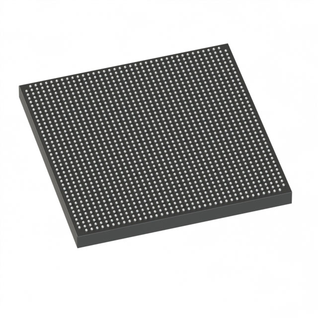
Stratix® V GX Field Programmable Gate Array (FPGA) IC 696 46080000 490000 1517-BBGA, FCBGA |
|---|---|
| Quantity | 1,421 Available (as of June 15, 2026) |
| Product Category | Field Programmable Gate Array (FPGA) |
|---|---|
| Manufacturer | Intel |
| Manufacturing Status | Obsolete |
| Manufacturer Standard Lead Time | Contact Us |
| Datasheet |
Specifications & Environmental
| Device Package | 1517-FBGA (40x40) | Grade | Industrial | Operating Temperature | -40°C – 100°C | ||
|---|---|---|---|---|---|---|---|
| Package / Case | 1517-BBGA, FCBGA | Number of I/O | 696 | Voltage | 820 mV - 880 mV | ||
| Mounting Method | Surface Mount | RoHS Compliance | RoHS Compliant | REACH Compliance | REACH Unknown | ||
| Moisture Sensitivity Level | 3 (168 Hours) | Number of LABs/CLBs | 185000 | Number of Logic Elements/Cells | 490000 | ||
| Number of Gates | N/A | ECCN | 3A001A2C | HTS Code | 8542.39.0001 | ||
| Qualification | N/A | Total RAM Bits | 46080000 |
Overview of 5SGXEA5K3F40I3LN – Stratix® V GX Field Programmable Gate Array (FPGA), 1517‑BBGA
The 5SGXEA5K3F40I3LN is a Stratix® V GX Field Programmable Gate Array (FPGA) in a 1517‑BBGA FCBGA package, offered as an industrial‑grade device. It provides high logic density and substantial embedded memory for complex, high‑bandwidth programmable logic implementations.
Designed for applications that require large on‑chip resources and extensive I/O, this device pairs approximately 490,000 logic elements with significant embedded RAM and a broad I/O count to support dense system integration and high‑speed interface implementation.
Key Features
- Logic Density — Approximately 490,000 logic elements supporting large, complex designs and extensive digital processing.
- Embedded Memory — Approximately 46 Mbits of on‑chip RAM to support large buffering, state storage, and memory‑intensive functions.
- I/O Capacity — Up to 696 I/Os to enable dense peripheral connectivity and multi‑interface systems.
- High‑speed Transceivers — Stratix V GX family transceiver speed grades are documented in the device datasheet; GX channel rates in the series include options up to 14.1 Gbps depending on transceiver and speed grade.
- Power and Core Voltage — Core supply range specified from 820 mV to 880 mV for predictable power‑domain design.
- Industrial Temperature Range — Rated for operation from −40 °C to 100 °C for reliable performance in industrial environments.
- Package & Mounting — 1517‑BBGA (FCBGA) package; supplier device package listed as 1517‑FBGA (40×40); surface‑mount mounting type for standard PCB assembly.
- Environmental Compliance — RoHS compliant.
Typical Applications
- High‑speed networking and communications — GX transceiver speed grades documented in the series enable implementation of multi‑Gbps interfaces where high bandwidth is required.
- Complex digital signal processing — Large logic element count and substantial on‑chip RAM support DSP, packet processing, and custom compute kernels.
- Dense I/O aggregation and protocol bridging — Up to 696 I/Os allow aggregation of numerous peripherals and protocol interfaces on a single device.
- Industrial systems and controls — Industrial temperature rating (−40 °C to 100 °C) suits deployment in harsh or temperature‑variable environments.
Unique Advantages
- High integration density: Approximately 490,000 logic elements reduce the need for multiple chips, simplifying system architecture and reducing BOM complexity.
- Large embedded memory: Approximately 46 Mbits of on‑chip RAM provides ample storage for buffering, state machines, and table lookups without external memory.
- Extensive I/O capability: 696 I/Os enable flexible interfacing and high channel counts for complex system designs.
- Industrial reliability: Specified operation from −40 °C to 100 °C supports deployment in challenging environments.
- Carefully specified power domain: Core voltage range (820–880 mV) helps with predictable power budgeting and thermal planning.
- RoHS compliance: Environmentally compliant manufacturing meets common regulatory requirements.
Why Choose 5SGXEA5K3F40I3LN?
The 5SGXEA5K3F40I3LN delivers a compelling combination of logic capacity, embedded memory, and I/O density in an industrial‑rated Stratix V GX FPGA package. Its resources are well suited to designs that demand large programmable logic arrays, significant on‑chip RAM, and high I/O counts while operating across a wide temperature range.
This device is appropriate for engineers and teams building high‑bandwidth communications equipment, complex signal processing systems, or dense interface aggregation solutions that require a robust, high‑resource FPGA platform with documented transceiver capabilities and clear electrical operating parameters.
Request a quote or submit an inquiry to receive pricing, availability, and lead‑time details for the 5SGXEA5K3F40I3LN.


Date Founded: 1968
Headquarters: Santa Clara, California, USA
Employees: 130,000+
Revenue: $54.23 Billion
Certifications and Memberships: ISO9001:2015, ISO14001:2015, ISO17025:2017, ISO27001:2022, ISO45001:2018, ISO50001:2018


