
5SGXEA5N2F45I3L
| Part Description |
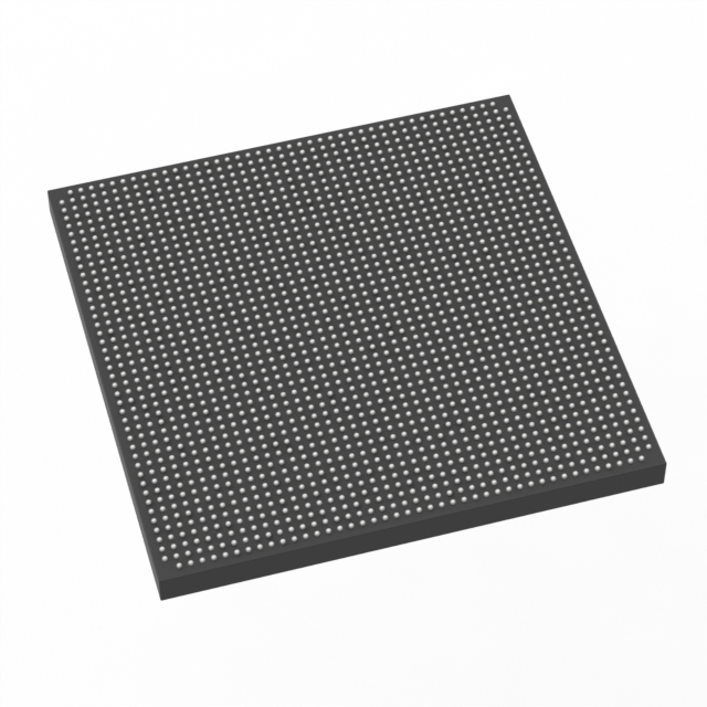
Stratix® V GX Field Programmable Gate Array (FPGA) IC 840 46080000 490000 1932-BBGA, FCBGA |
|---|---|
| Quantity | 867 Available (as of June 10, 2026) |

| Product Category | Field Programmable Gate Array (FPGA) |
|---|---|
| Manufacturer | Intel |
| Manufacturing Status | Obsolete |
| Manufacturer Standard Lead Time | Contact Us |
| Datasheet |
Specifications & Environmental
| Device Package | 1932-FBGA, FC (45x45) | Grade | Industrial | Operating Temperature | -40°C – 100°C | ||
|---|---|---|---|---|---|---|---|
| Package / Case | 1932-BBGA, FCBGA | Number of I/O | 840 | Voltage | 820 mV - 880 mV | ||
| Mounting Method | Surface Mount | RoHS Compliance | RoHS Compliant | REACH Compliance | REACH Unknown | ||
| Moisture Sensitivity Level | 3 (168 Hours) | Number of LABs/CLBs | 185000 | Number of Logic Elements/Cells | 490000 | ||
| Number of Gates | N/A | ECCN | 3A001A2C | HTS Code | 8542.39.0001 | ||
| Qualification | N/A | Total RAM Bits | 46080000 |
Overview of 5SGXEA5N2F45I3L – Stratix® V GX FPGA, approximately 490,000 logic elements, 840 I/Os
The 5SGXEA5N2F45I3L is a Stratix® V GX field programmable gate array (FPGA) IC from Intel, offered in an industrial temperature grade. It delivers large programmable logic capacity and extensive I/O in a high-density FCBGA package for demanding embedded and communications applications.
Designed as part of the Stratix V GX family, the device provides abundant on-chip memory and I/O resources, a low-voltage core supply range, and support for Stratix V transceiver speed grades as documented in the device datasheet.
Key Features
- Logic Capacity Approximately 490,000 logic elements to implement complex custom logic and large-scale designs.
- Embedded Memory Approximately 46 Mbits of on-chip RAM to support buffering, packet processing, and on-chip data storage.
- I/O Resources 840 I/O pins to enable high-connectivity designs and dense external interfacing.
- Transceiver Support (Stratix V GX family) Stratix V GX devices include transceiver speed-grade options documented in the datasheet (up to 14.1 Gbps in applicable GX grades), enabling high-bandwidth serial links where required.
- Power and Core Voltage Core voltage supply range of 820 mV to 880 mV to match system power delivery requirements for Stratix V devices.
- Package 1932-BBGA FCBGA (supplier package: 1932-FBGA, FC 45×45) in a surface-mount form factor for compact board-level integration.
- Temperature and Grade Industrial temperature range from –40 °C to 100 °C and industrial grade designation for deployment in temperature-demanding environments.
- RoHS Compliance RoHS compliant to support environmental restriction requirements.
Typical Applications
- High‑speed communications and networking Supports designs that require large logic fabrics, abundant memory, and Stratix V GX transceiver speed grades for high-bandwidth serial links.
- Signal processing and FPGA acceleration Large logic capacity and on-chip RAM enable implementation of complex DSP pipelines and custom accelerators.
- Prototyping and system integration High I/O count and dense logic resources make the device suitable for large prototype boards and system-level integration.
- Test and measurement equipment Industrial temperature rating and plentiful I/O allow deployment in instrument and test systems operating across wide temperature ranges.
Unique Advantages
- High logic density: Approximately 490,000 logic elements let you implement large, complex designs on a single device, reducing the need for multi‑device solutions.
- Substantial embedded memory: Around 46 Mbits of on-chip RAM supports deep buffering and stateful processing without reliance on external memory.
- Extensive I/O connectivity: 840 I/Os provide flexible interfacing options for high-pin-count systems and dense peripheral connectivity.
- Industrial temperature capability: Rated from –40 °C to 100 °C for deployment in temperature-challenging environments.
- Compact high-density package: 1932-BBGA FCBGA package enables high integration density on modern PCBs while remaining surface-mount compatible.
- Documented Stratix V GX transceiver options: Family-level transceiver speed grades are provided in the Stratix V datasheet for high-bandwidth serial link designs.
Why Choose 5SGXEA5N2F45I3L?
The 5SGXEA5N2F45I3L sits in the Stratix V GX family to deliver a balance of large programmable logic capacity, significant embedded memory, and high I/O density in a single industrial-grade FCBGA package. It is suited to engineers implementing complex, high-throughput designs that require on-chip resources and robust temperature performance.
Backed by Intel/Altera Stratix V device documentation, this part is appropriate for teams seeking scalable FPGA resources with clear electrical and timing characteristics documented in the device datasheet.
Request a quote or submit an inquiry to discuss pricing, availability, and technical requirements for the 5SGXEA5N2F45I3L.


Date Founded: 1968
Headquarters: Santa Clara, California, USA
Employees: 130,000+
Revenue: $54.23 Billion
Certifications and Memberships: ISO9001:2015, ISO14001:2015, ISO17025:2017, ISO27001:2022, ISO45001:2018, ISO50001:2018


