
5SGXEA7H1F35C1
| Part Description |
Stratix® V GX Field Programmable Gate Array (FPGA) IC 552 51200000 622000 1152-BBGA, FCBGA |
|---|---|
| Quantity | 25 Available (as of June 15, 2026) |

| Product Category | Field Programmable Gate Array (FPGA) |
|---|---|
| Manufacturer | Intel |
| Manufacturing Status | Obsolete |
| Manufacturer Standard Lead Time | Contact Us |
| Datasheet |
Specifications & Environmental
| Device Package | 1152-FBGA (35x35) | Grade | Commercial | Operating Temperature | 0°C – 85°C | ||
|---|---|---|---|---|---|---|---|
| Package / Case | 1152-BBGA, FCBGA | Number of I/O | 552 | Voltage | 870 mV - 930 mV | ||
| Mounting Method | Surface Mount | RoHS Compliance | RoHS Compliant | REACH Compliance | REACH Unknown | ||
| Moisture Sensitivity Level | 3 (168 Hours) | Number of LABs/CLBs | 234720 | Number of Logic Elements/Cells | 622000 | ||
| Number of Gates | N/A | ECCN | 3A001A2C | HTS Code | 8542.39.0001 | ||
| Qualification | N/A | Total RAM Bits | 51200000 |
Overview of 5SGXEA7H1F35C1 – Stratix® V GX Field Programmable Gate Array (FPGA) IC
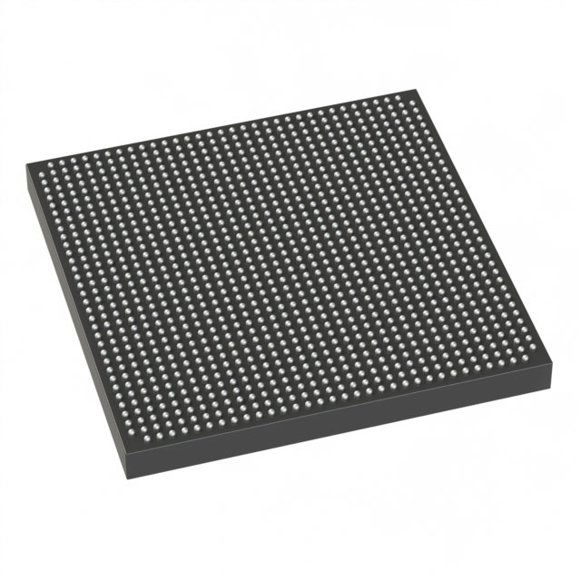
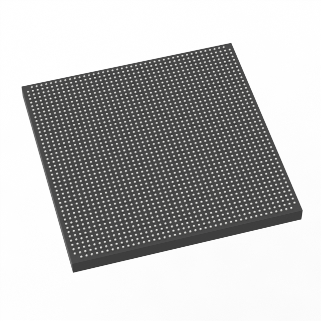
The 5SGXEA7H1F35C1 is a Stratix V GX Field Programmable Gate Array from Intel, offered in a commercial temperature grade. This high-density FPGA delivers large on-chip logic and memory resources with a broad I/O complement, packaged in a 1152-ball FCBGA suitable for surface-mount assembly.
Engineered for designs that require significant programmable logic capacity, substantial embedded memory, and extensive I/O, this device addresses demanding digital designs where integration and predictable supply and thermal envelopes are important.
Key Features
- Logic Capacity 622,000 logic elements provide substantial programmable logic resources for complex digital designs.
- Embedded Memory Approximately 51.2 Mbits of on-chip RAM for large buffering, lookup tables, and data storage close to logic.
- I/O Density 552 I/O pins support high-connectivity designs and extensive external interfacing.
- Power and Core Supply Specified core voltage range of 870 mV to 930 mV for regulated power planning and supply design.
- Package & Mounting 1152-BBGA (FCBGA) 35×35 supplier package in a surface-mount form factor for high-density PCB integration.
- Temperature Grade Commercial operating range of 0°C to 85°C suitable for standard commercial electronics environments.
- Environmental Compliance RoHS compliant for global manufacturing and regulatory alignment.
- Stratix V GX Family Part of the Stratix V GX family; the series documentation describes configurable core and transceiver speed grade options at the family level.
Typical Applications
- High-density programmable logic — Utilize the device’s 622,000 logic elements for complex state machines, pipelined datapaths, and custom accelerators where large logic capacity is required.
- On-chip buffering and memory-intensive functions — Approximately 51.2 Mbits of embedded RAM enables large FIFOs, caches, and local data storage to minimize external memory dependency.
- High-pin-count interfacing — 552 I/O pins support systems requiring wide parallel interfaces, multiple high-speed links, or extensive peripheral connectivity.
Unique Advantages
- Substantial programmable logic: 622,000 logic elements let designers implement complex, high‑parallelism architectures without immediate migration to multi-FPGA systems.
- Large on-chip memory: Approximately 51.2 Mbits of embedded RAM reduce the need for external memory and lower system latency for data‑intensive functions.
- Broad I/O support: 552 I/Os enable flexible board-level interfacing and consolidation of multiple signals onto a single device.
- Controlled core supply range: Defined core voltage between 870 mV and 930 mV simplifies power‑rail planning and component selection.
- Commercial-ready packaging: 1152-ball FCBGA (35×35) surface-mount package supports compact, high-density PCB layouts for commercial electronics.
- Regulatory alignment: RoHS compliance supports environmentally responsible manufacturing and global market access.
Why Choose 5SGXEA7H1F35C1?
The 5SGXEA7H1F35C1 combines very large programmable logic resources with substantial embedded memory and high I/O density in a commercial-grade Stratix V GX package. Its well-defined core voltage range and surface-mount FCBGA packaging make it suitable for high-integration, high-capacity designs where minimizing external components and maximizing on-chip resources are priorities.
This part is appropriate for engineering teams developing complex digital systems that require scalable logic, significant on-chip RAM, and abundant external connectivity while operating within standard commercial environmental conditions. The device’s placement within the Stratix V GX family aligns it with the family-level capabilities documented in the series datasheet.
Request a quote or submit an inquiry to receive pricing, availability, and technical support information for 5SGXEA7H1F35C1.


Date Founded: 1968
Headquarters: Santa Clara, California, USA
Employees: 130,000+
Revenue: $54.23 Billion
Certifications and Memberships: ISO9001:2015, ISO14001:2015, ISO17025:2017, ISO27001:2022, ISO45001:2018, ISO50001:2018


