
5SGXEA7K2F35C1N
| Part Description |
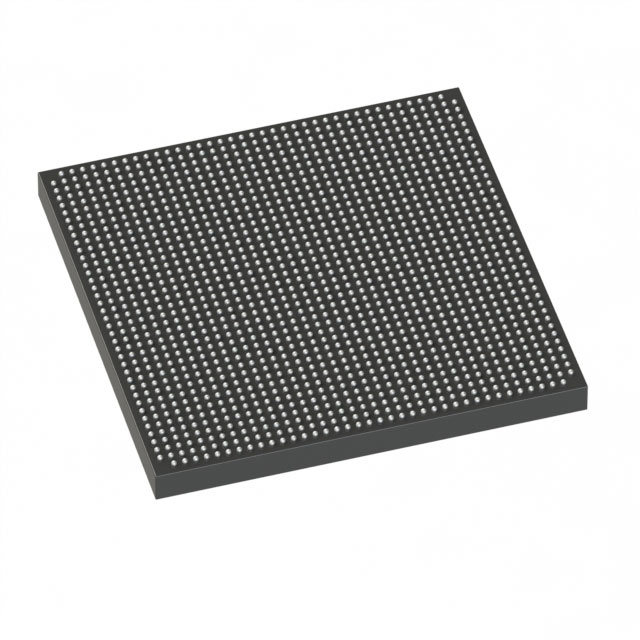
Stratix® V GX Field Programmable Gate Array (FPGA) IC 432 51200000 622000 1152-BBGA, FCBGA |
|---|---|
| Quantity | 990 Available (as of June 14, 2026) |

| Product Category | Field Programmable Gate Array (FPGA) |
|---|---|
| Manufacturer | Intel |
| Manufacturing Status | Obsolete |
| Manufacturer Standard Lead Time | Contact Us |
| Datasheet |
Specifications & Environmental
| Device Package | 1152-FBGA (35x35) | Grade | Commercial | Operating Temperature | 0°C – 85°C | ||
|---|---|---|---|---|---|---|---|
| Package / Case | 1152-BBGA, FCBGA | Number of I/O | 432 | Voltage | 870 mV - 930 mV | ||
| Mounting Method | Surface Mount | RoHS Compliance | RoHS Compliant | REACH Compliance | REACH Unknown | ||
| Moisture Sensitivity Level | 3 (168 Hours) | Number of LABs/CLBs | 234720 | Number of Logic Elements/Cells | 622000 | ||
| Number of Gates | N/A | ECCN | 3A001A2C | HTS Code | 8542.39.0001 | ||
| Qualification | N/A | Total RAM Bits | 51200000 |
Overview of 5SGXEA7K2F35C1N – Stratix® V GX FPGA, 622,000 logic elements, ~51.2 Mbits RAM, 432 I/Os, 1152-BBGA
The 5SGXEA7K2F35C1N is a Stratix® V GX Field Programmable Gate Array (FPGA) offered in a 1152-BBGA surface-mount package. The device delivers 622,000 logic elements and approximately 51.2 Mbits of embedded memory, providing substantial on-chip resources for complex programmable logic designs.
As a commercial-grade Stratix V GX device, it operates with a core supply range of 0.870 V to 0.930 V and an ambient temperature range of 0 °C to 85 °C. Series-level documentation for Stratix V GX devices includes electrical and switching characteristics and transceiver-related details useful for system-level planning.
Key Features
- Logic Capacity 622,000 logic elements for integrating extensive programmable logic on a single device.
- Embedded Memory Approximately 51.2 Mbits of on-chip RAM to support buffering, state storage, and memory-intensive logic.
- I/O and Packaging 432 I/Os with a 1152-BBGA package (supplier device package: 1152-FBGA, 35×35) optimized for surface-mount assembly.
- Power Core supply voltage range of 870 mV to 930 mV to match low-voltage FPGA power domains.
- Temperature and Grade Commercial temperature grade rated for operation from 0 °C to 85 °C.
- Compliance RoHS compliant for environmental compliance in commercial applications.
Typical Applications
- I/O‑dense system integration Designs that require a high number of direct I/Os can leverage the device’s 432 I/O pins to minimize external multiplexing.
- Large on-chip logic implementations Systems needing substantial programmable logic capacity can consolidate functions using the 622,000 logic elements.
- Memory‑heavy designs Applications that benefit from significant on-chip RAM for buffering or state machines can use the approximately 51.2 Mbits of embedded memory.
- Commercial electronic products Products and prototypes intended for commercial temperature environments (0 °C to 85 °C) and standard RoHS compliance.
Unique Advantages
- High logic density: 622,000 logic elements enable consolidation of complex functions on a single FPGA, reducing the need for multiple devices.
- Substantial on-chip memory: Approximately 51.2 Mbits of embedded RAM reduces dependence on external memory components and simplifies board design.
- Generous I/O count: 432 I/Os provide flexible interfacing for parallel buses, peripherals, and multiple interfaces without extensive external logic.
- Compact BGA package: 1152-BBGA (supplier 1152-FBGA, 35×35) surface-mount format supports dense PCB layouts and industry-standard assembly workflows.
- Low-voltage core operation: 0.870–0.930 V supply range aligns with contemporary low-voltage FPGA core domains and power-management strategies.
- Commercial readiness and compliance: Rated for 0 °C to 85 °C and RoHS compliant for deployment in commercial electronic products.
Why Choose 5SGXEA7K2F35C1N?
The 5SGXEA7K2F35C1N positions itself as a high-capacity, commercially graded Stratix V GX FPGA that combines large logic resources, significant embedded memory, and a high I/O count in a compact 1152-BBGA surface-mount package. Its electrical characteristics and series-level documentation support system designers in planning power, I/O timing, and device-level integration.
This device is well-suited for design teams and integrators who require dense programmable logic and on-chip memory within a commercial temperature envelope and standard RoHS compliance. The part offers a clear path for consolidating complex functions onto a single FPGA while retaining flexibility for board-level implementation.
Request a quote or submit a pricing and availability inquiry to begin evaluating 5SGXEA7K2F35C1N for your next design project.


Date Founded: 1968
Headquarters: Santa Clara, California, USA
Employees: 130,000+
Revenue: $54.23 Billion
Certifications and Memberships: ISO9001:2015, ISO14001:2015, ISO17025:2017, ISO27001:2022, ISO45001:2018, ISO50001:2018


