
5SGXEA7K2F35C2G
| Part Description |
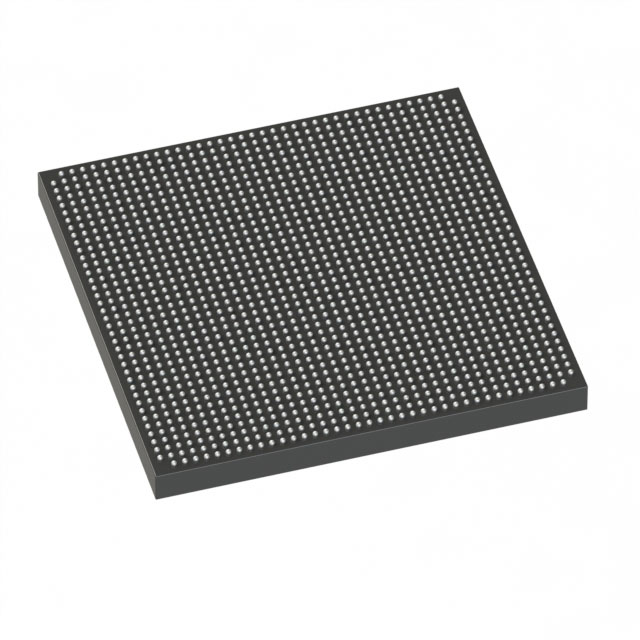
Stratix® V GX Field Programmable Gate Array (FPGA) IC 432 51200000 622000 1152-BBGA, FCBGA |
|---|---|
| Quantity | 295 Available (as of June 10, 2026) |

| Product Category | Field Programmable Gate Array (FPGA) |
|---|---|
| Manufacturer | Intel |
| Manufacturing Status | Active |
| Manufacturer Standard Lead Time | 26 Weeks |
| Datasheet |
Specifications & Environmental
| Device Package | 1152-FBGA (35x35) | Grade | Commercial | Operating Temperature | 0°C – 85°C | ||
|---|---|---|---|---|---|---|---|
| Package / Case | 1152-BBGA, FCBGA | Number of I/O | 432 | Voltage | 870 mV - 930 mV | ||
| Mounting Method | Surface Mount | RoHS Compliance | RoHS Compliant | REACH Compliance | REACH Unaffected | ||
| Moisture Sensitivity Level | 3 (168 Hours) | Number of LABs/CLBs | 234720 | Number of Logic Elements/Cells | 622000 | ||
| Number of Gates | N/A | ECCN | N/A | HTS Code | N/A | ||
| Qualification | N/A | Total RAM Bits | 51200000 |
Overview of 5SGXEA7K2F35C2G – Stratix® V GX FPGA, 622,000 logic elements, ~51.2 Mbits RAM, 432 I/O
The 5SGXEA7K2F35C2G is a Stratix V GX field programmable gate array (FPGA) designed for commercial applications requiring large logic capacity, substantial on-chip memory, and broad I/O connectivity. Built on the Stratix V GX device family, this device addresses designs that need high integration of programmable logic, embedded RAM, and transceiver-capable architecture as described for the Stratix V series.
Key value for designers comes from a combination of high logic density, significant embedded memory, and a 1152-ball BGA package suitable for surface-mount assembly, enabling compact high-performance boards within the commercial temperature range.
Key Features
- Core Logic Capacity Provides 622,000 logic elements for complex digital designs and high-density implementations.
- Embedded Memory Approximately 51.2 Mbits of on-chip RAM to support large buffers, FIFOs, and on-chip data structures.
- I/O Resources 432 device I/Os to support wide parallel interfaces, multi-channel connectivity, and extensive board-level interfacing.
- Package 1152-ball BGA, FCBGA (supplier package: 1152-FBGA, 35 × 35 mm) optimized for surface-mount PCB assembly and high-density routing.
- Power Core supply range specified at 870 mV to 930 mV for the device core power rail.
- Operating Range Commercial grade with an operating temperature range of 0 °C to 85 °C.
- Mounting Surface-mount device suitable for modern PCB manufacturing processes.
- Compliance RoHS compliant.
- Series Characteristics Part of the Stratix V family with documented electrical and switching characteristics, including transceiver specifications and programmable I/O timing (see series datasheet for details).
Typical Applications
- High-speed communications Appropriate for designs that leverage the Stratix V GX series transceiver capabilities and rich I/O set to implement multi-channel communication interfaces and protocol engines.
- Data processing and acceleration Large logic capacity and abundant on-chip RAM enable hardware acceleration, packet processing, and custom data-path implementations.
- Prototyping and complex system integration High-density logic and memory resources support system prototyping where integration of multiple functions into a single FPGA reduces board-level complexity.
Unique Advantages
- High logic density: 622,000 logic elements allow consolidation of complex functions and large finite-state machines into a single device, reducing BOM and interconnect complexity.
- Substantial on-chip memory: Approximately 51.2 Mbits of embedded RAM supports large buffering and local data storage, minimizing external memory needs.
- Extensive I/O: 432 I/Os enable wide parallel interfaces, multiple peripheral connections, and flexible board partitioning.
- Compact BGA package: 1152-ball FCBGA (35 × 35 mm) offers a compact form factor for high-density PCB designs while supporting surface-mount assembly processes.
- Commercial temperature and RoHS compliance: Rated for 0 °C to 85 °C operation and RoHS compliant to meet commercial production requirements.
- Defined core power range: Core voltage specified between 870 mV and 930 mV to guide power-supply design and ensure predictable power characteristics.
Why Choose 5SGXEA7K2F35C2G?
The 5SGXEA7K2F35C2G combines high logic capacity, significant embedded RAM, and extensive I/O in a compact 1152-ball BGA package, positioning it for commercial designs that demand integrated programmable logic and memory resources. It is suitable for teams implementing complex data-paths, communication interfaces, and system-level functions where board-level consolidation and predictable electrical characteristics are important.
As a member of the Stratix V GX family, this device benefits from the series’ documented electrical and switching characteristics, enabling designers to align device selection with system performance targets while leveraging established device documentation for implementation details.
Request a quote or submit a pricing inquiry to evaluate 5SGXEA7K2F35C2G for your next high-density FPGA design.


Date Founded: 1968
Headquarters: Santa Clara, California, USA
Employees: 130,000+
Revenue: $54.23 Billion
Certifications and Memberships: ISO9001:2015, ISO14001:2015, ISO17025:2017, ISO27001:2022, ISO45001:2018, ISO50001:2018


