
5SGXEA7K2F35C1G
| Part Description |
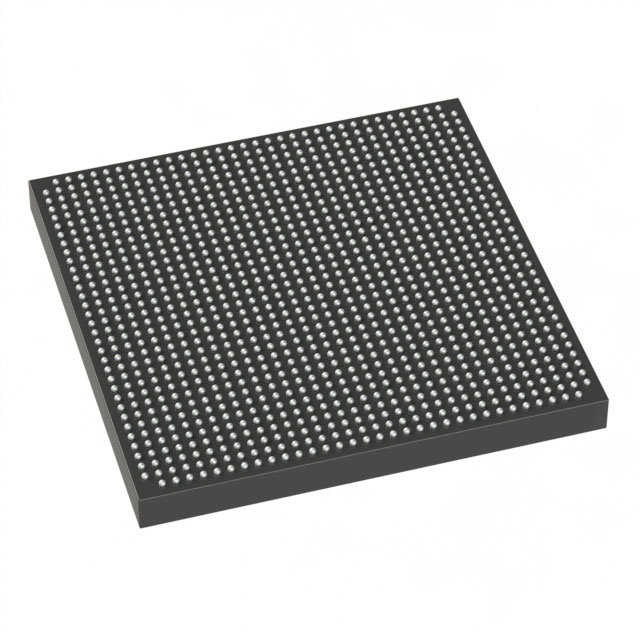
Stratix® V GX Field Programmable Gate Array (FPGA) IC 432 51200000 622000 1152-BBGA, FCBGA |
|---|---|
| Quantity | 325 Available (as of June 15, 2026) |
| Product Category | Field Programmable Gate Array (FPGA) |
|---|---|
| Manufacturer | Intel |
| Manufacturing Status | Active |
| Manufacturer Standard Lead Time | 26 Weeks |
| Datasheet |
Specifications & Environmental
| Device Package | 1152-FBGA (35x35) | Grade | Commercial | Operating Temperature | 0°C – 85°C | ||
|---|---|---|---|---|---|---|---|
| Package / Case | 1152-BBGA, FCBGA | Number of I/O | 432 | Voltage | 870 mV - 930 mV | ||
| Mounting Method | Surface Mount | RoHS Compliance | RoHS Compliant | REACH Compliance | REACH Unaffected | ||
| Moisture Sensitivity Level | 3 (168 Hours) | Number of LABs/CLBs | 234720 | Number of Logic Elements/Cells | 622000 | ||
| Number of Gates | N/A | ECCN | N/A | HTS Code | N/A | ||
| Qualification | N/A | Total RAM Bits | 51200000 |
Overview of 5SGXEA7K2F35C1G – Stratix V GX Field Programmable Gate Array (FPGA)
The 5SGXEA7K2F35C1G is a Stratix® V GX Field Programmable Gate Array (FPGA) in a 1152-BBGA FCBGA package from Intel. This commercial-grade device delivers very large logic capacity, significant embedded RAM, and a high I/O count for complex system designs that require dense programmable logic and on-chip memory.
Designed for applications that demand high integration, the device pairs 622,000 logic elements with approximately 51.2 Mbits of embedded memory and 432 I/Os, enabling consolidation of multiple functions into a single FPGA while supporting surface-mount assembly in a 1152-pin BGA footprint.
Key Features
- Core Logic 622,000 logic elements (logic cells) provide substantial programmable fabric for complex algorithms, state machines, and custom accelerators.
- Embedded Memory Approximately 51.2 Mbits of on-chip RAM supports large buffering, FIFOs, and memory-intensive logic without external memory dependence.
- I/O Capacity 432 I/Os accommodate wide parallel buses, multiple interfaces, and diverse peripheral connections in a single device.
- Power Voltage supply range of 870 mV to 930 mV suitable for the device’s operating requirements as specified.
- Package & Mounting 1152-BBGA, FCBGA package (supplier device package: 1152-FBGA, 35×35) in a surface-mount form factor for high-density board integration.
- Temperature & Grade Commercial-grade device rated for 0 °C to 85 °C operation.
- Regulatory RoHS compliant for environmental and manufacturing compatibility.
Typical Applications
- High-density logic integration Implement complex state machines, protocol engines, and custom datapaths using the large pool of logic elements.
- Memory-intensive processing On-chip RAM enables buffering, packet memory, and signal-processing data storage without immediate reliance on external memories.
- Systems with large I/O requirements Support multiple parallel interfaces, sensor arrays, or wide data buses with 432 available I/Os.
- Compact board designs Surface-mount 1152-BBGA package allows dense PCB layouts and consolidation of functions into a single FPGA component.
Unique Advantages
- Extensive logic capacity: 622,000 logic elements let you implement large-scale digital designs on a single device, reducing board-level complexity.
- Substantial embedded memory: Approximately 51.2 Mbits of on-chip RAM supports large FIFOs, buffering, and local data storage to improve system throughput.
- High I/O count: 432 I/Os provide flexibility for interfacing multiple peripherals and parallel data paths without external expansion.
- Compact, manufacturable package: 1152-pin BGA (35×35) surface-mount package supports modern PCB assembly and high-density system integration.
- Commercial temperature rating: Specified 0 °C to 85 °C operating range aligns with many embedded and commercial electronics designs.
- RoHS compliant: Facilitates compliance with environmental manufacturing requirements.
Why Choose 5SGXEA7K2F35C1G?
The 5SGXEA7K2F35C1G positions itself as a high-capacity Stratix V GX FPGA option for designers who need large programmable logic resources, substantial on-chip memory, and a high count of I/Os within a compact BGA package. Its combination of 622,000 logic elements, approximately 51.2 Mbits of embedded RAM, and 432 I/Os makes it suitable for consolidating multiple system functions onto a single device, simplifying BOMs and board layouts.
This commercial-grade FPGA is appropriate for teams building complex embedded systems, communications interfaces, or high-density digital logic designs that require a balance of logic, memory, and I/O in a surface-mount 1152-pin package. The Intel Stratix V GX family support and documentation help ensure long-term design continuity and scalability within the same device family.
Request a quote or submit an inquiry to get pricing, availability, and ordering information for 5SGXEA7K2F35C1G.


Date Founded: 1968
Headquarters: Santa Clara, California, USA
Employees: 130,000+
Revenue: $54.23 Billion
Certifications and Memberships: ISO9001:2015, ISO14001:2015, ISO17025:2017, ISO27001:2022, ISO45001:2018, ISO50001:2018


