
5SGXEA7K2F35I2L
| Part Description |
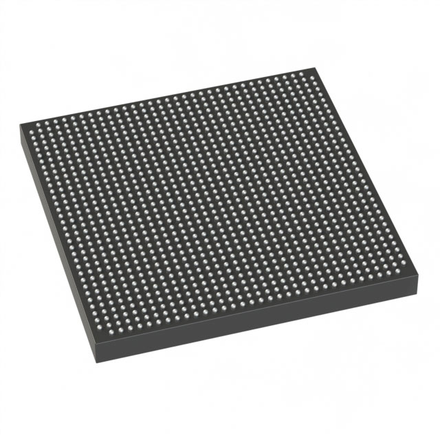
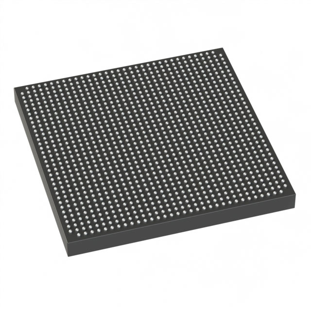
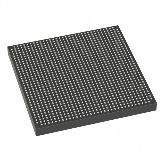
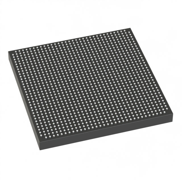
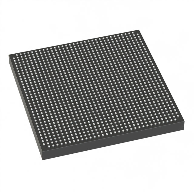
Stratix® V GX Field Programmable Gate Array (FPGA) IC 432 51200000 622000 1152-BBGA, FCBGA |
|---|---|
| Quantity | 772 Available (as of October 7, 2026) |
| Product Category | Field Programmable Gate Array (FPGA) |
|---|---|
| Manufacturer | Intel |
| Manufacturing Status | Obsolete |
| Manufacturer Standard Lead Time | Contact Us |
| Datasheet |
Specifications & Environmental
| Device Package | 1152-FBGA (35x35) | Grade | Industrial | Operating Temperature | -40°C – 100°C | ||
|---|---|---|---|---|---|---|---|
| Package / Case | 1152-BBGA, FCBGA | Number of I/O | 432 | Voltage | 820 mV - 880 mV | ||
| Mounting Method | Surface Mount | RoHS Compliance | RoHS Compliant | REACH Compliance | REACH Unknown | ||
| Moisture Sensitivity Level | 3 (168 Hours) | Number of LABs/CLBs | 234720 | Number of Logic Elements/Cells | 622000 | ||
| Number of Gates | N/A | ECCN | 3A001A2C | HTS Code | 8542.39.0001 | ||
| Qualification | N/A | Total RAM Bits | 51200000 |
Overview of 5SGXEA7K2F35I2L – Stratix® V GX FPGA, 622,000 Logic Elements, ~51.2 Mbits RAM, 1152-BBGA
The 5SGXEA7K2F35I2L is a Stratix V GX field-programmable gate array (FPGA) from Intel designed for high‑density, high‑I/O applications. It combines large logic capacity, substantial embedded memory, and a high I/O count in a single surface-mount FCBGA package targeted at industrial-grade designs.
With family-level support for high-speed transceiver operation and an industrial operating temperature range, this device addresses applications that require significant on‑chip resources and robust environmental performance.
Key Features
- Logic Capacity 622,000 logic elements and 234,720 logic array blocks (LABs) provide extensive programmable fabric for complex logic and custom acceleration.
- Embedded Memory Approximately 51.2 Mbits of total on‑chip RAM to support large buffers, LUT-based engines, and state storage without external memory in many designs.
- I/O Resources 432 user I/O pins to interface with high-pin-count peripherals, multi-lane SERDES arrangements, and dense board-level connectivity.
- Power and Core Voltage Core supply range specified at 820 mV to 880 mV to meet the device’s defined operating conditions.
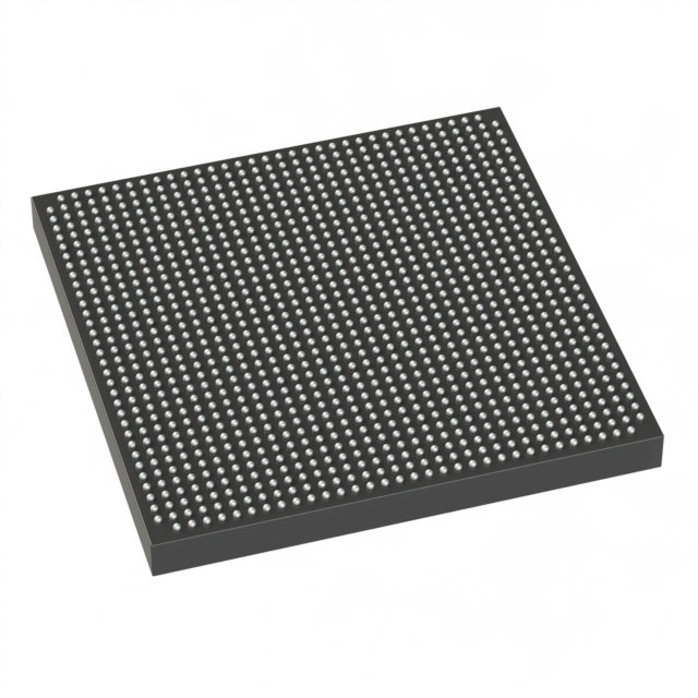
- Package and Mounting 1152-BBGA (FCBGA) package; supplier device package listed as 1152-FBGA (35 × 35). Surface-mount mounting type for standard PCB assembly.
- Temperature Grade Industrial grade with an operating temperature range of −40 °C to 100 °C for deployments in demanding environments.
- Compliance RoHS‑compliant for regulatory alignment in lead‑free assemblies.
- Stratix V GX Family Transceiver Support Stratix V GX family devices include transceiver speed grades; consult the Stratix V device datasheet for supported channel rates and speed‑grade options.
Typical Applications
- High‑performance data processing Large logic and memory resources enable compute‑intensive algorithms, packet processing, and custom accelerators implemented on‑chip.
- High‑density I/O systems The 432 I/O pins support multi‑channel interfaces, board‑level aggregation, and dense peripheral connectivity.
- Industrial and ruggedized equipment Industrial temperature rating (−40 °C to 100 °C) makes the device suitable for controls, instrumentation, and other industrial deployments.
- High‑speed serial links (family support) As a Stratix V GX family device, it aligns with applications that require high‑speed transceivers; refer to the Stratix V datasheet for specific transceiver speed options.
Unique Advantages
- High integration density: 622,000 logic elements and ~51.2 Mbits of embedded RAM reduce dependence on external logic and memory, simplifying system design.
- Robust I/O capability: 432 I/Os allow extensive peripheral interfacing and support for multi‑lane I/O architectures without additional multiplexing hardware.
- Industrial temperature range: Rated for −40 °C to 100 °C operation, enabling reliable performance in challenging environmental conditions.
- Compact BGA footprint: 1152‑ball FCBGA package provides a high pin count in a compact footprint for space‑constrained PCBs.
- Standards‑aligned manufacturing: Surface-mount package and RoHS compliance streamline modern assembly and regulatory requirements.
- Family documentation and support: Backed by the Stratix V device datasheet and Intel’s device documentation for electrical, timing, and transceiver guidance.
Why Choose 5SGXEA7K2F35I2L?
The 5SGXEA7K2F35I2L delivers a combination of high logic and memory capacity, substantial I/O resources, and industrial temperature capability in a single Stratix V GX FPGA package. It is positioned for complex, resource‑intensive designs where on‑chip logic and memory density, combined with robust environmental performance, are primary requirements.
Designers targeting industrial systems, high‑density I/O applications, or projects that leverage the Stratix V family transceiver options will find this device well suited for scalable, long‑lifecycle deployments backed by Intel’s Stratix V documentation.
Request a quote or submit an inquiry to receive pricing and availability information for 5SGXEA7K2F35I2L. Technical sales can provide lead times, volume pricing, and support materials to assist with evaluation and procurement.





















Date Founded: 1968
Headquarters: Santa Clara, California, USA
Employees: 130,000+
Revenue: $54.23 Billion
Certifications and Memberships: ISO9001:2015, ISO14001:2015, ISO17025:2017, ISO27001:2022, ISO45001:2018, ISO50001:2018


