
5SGXEA7K2F40C1N
| Part Description |
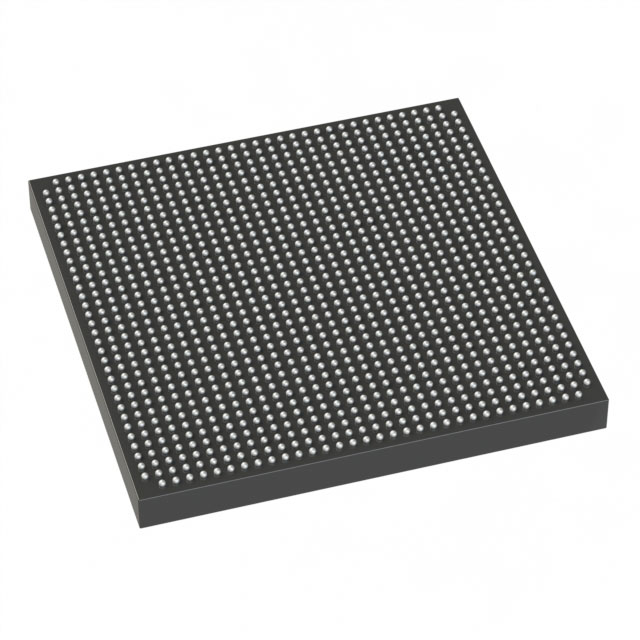
Stratix® V GX Field Programmable Gate Array (FPGA) IC 696 51200000 622000 1517-BBGA, FCBGA |
|---|---|
| Quantity | 1,099 Available (as of June 18, 2026) |

| Product Category | Field Programmable Gate Array (FPGA) |
|---|---|
| Manufacturer | Intel |
| Manufacturing Status | Obsolete |
| Manufacturer Standard Lead Time | Contact Us |
| Datasheet |
Specifications & Environmental
| Device Package | 1517-FBGA (40x40) | Grade | Commercial | Operating Temperature | 0°C – 85°C | ||
|---|---|---|---|---|---|---|---|
| Package / Case | 1517-BBGA, FCBGA | Number of I/O | 696 | Voltage | 870 mV - 930 mV | ||
| Mounting Method | Surface Mount | RoHS Compliance | RoHS Compliant | REACH Compliance | REACH Unknown | ||
| Moisture Sensitivity Level | 3 (168 Hours) | Number of LABs/CLBs | 234720 | Number of Logic Elements/Cells | 622000 | ||
| Number of Gates | N/A | ECCN | 3A001A2C | HTS Code | 8542.39.0001 | ||
| Qualification | N/A | Total RAM Bits | 51200000 |
Overview of 5SGXEA7K2F40C1N – Stratix® V GX FPGA, 622,000 logic elements
The 5SGXEA7K2F40C1N is a Stratix® V GX field programmable gate array (FPGA) from Intel, supplied in a 1517-BBGA FCBGA package. It delivers high device density and on-chip memory with dedicated multi-gigabit transceiver support provided by the Stratix V GX family.
Designed for commercial-temperature applications, this device targets high-density programmable logic and high-speed serial interfaces where large logic capacity, abundant I/O, and significant embedded memory are required.
Key Features
- Core Logic Approximately 622,000 logic elements to implement large-scale programmable logic functions.
- Logic Blocks 234,720 logic blocks (as provided in product data) to structure complex designs across the fabric.
- Embedded Memory Approximately 51.2 Mbits of on-chip RAM for buffering, packet queues, and on-chip data storage.
- I/O Density 696 general-purpose I/Os to connect multiple peripherals, memory interfaces, and board-level signals.
- Transceiver Family Capability Part of the Stratix V GX family, which the datasheet documents with GX transceiver speed grades up to 14.1 Gbps (series-level specification).
- Power and Supply Core voltage supply range specified from 870 mV to 930 mV, enabling controlled power design for the FPGA core.
- Package & Mounting 1517-BBGA (FCBGA) package; supplier device package listed as 1517-FBGA (40×40). Surface-mount device for high-density PCB assembly.
- Operating Grade & Temperature Commercial grade with an operating temperature range of 0 °C to 85 °C.
- Compliance RoHS compliant.
Typical Applications
- High-density programmable logic Large designs that require substantial logic resources and on-chip memory can be mapped onto the device’s 622,000 logic elements and ~51.2 Mbits of RAM.
- High-speed serial interfaces As a Stratix V GX family device, it supports multi-gigabit transceiver speed grades documented for GX devices, suitable for designs requiring high-speed links.
- Complex I/O integration With 696 I/Os, the FPGA can consolidate multiple board-level interfaces, reducing component count in systems that require many signals.
Unique Advantages
- High logic capacity: Enables implementation of complex, feature-rich designs in a single device, minimizing the need for device partitioning.
- Significant on-chip memory: Approximately 51.2 Mbits of embedded RAM supports buffering, packet handling, and data-path staging without external memory for many functions.
- Large I/O complement: 696 I/Os allow dense system integration and flexible interfacing to peripherals, memory, and ASICs.
- Stratix V GX series transceiver support: Series-level transceiver speed grades are documented in the device family datasheet, enabling multi-gigabit serial designs when appropriate speed grades are selected.
- Commercial-grade temperature range: Rated 0 °C to 85 °C for typical commercial environments and system-level deployments.
- RoHS compliant: Conforms to RoHS requirements for environmental and regulatory compatibility in commercial products.
Why Choose 5SGXEA7K2F40C1N?
The 5SGXEA7K2F40C1N positions itself as a high-density Stratix® V GX FPGA solution for commercial designs that need extensive logic resources, substantial embedded memory, and a high I/O count. Its family-level transceiver capabilities make it suitable for designs incorporating multi-gigabit serial links, while the FCBGA 1517 package supports high-density board integration.
Engineers and procurement teams seeking a commercial-grade, RoHS-compliant FPGA with measurable, verifiable specifications—622,000 logic elements, ~51.2 Mbits of RAM, 696 I/Os, and a defined core voltage and temperature range—will find this part suitable for complex, integrated digital and high-speed interface applications.
Request a quote or submit an inquiry to receive pricing, availability, and technical support information for 5SGXEA7K2F40C1N.


Date Founded: 1968
Headquarters: Santa Clara, California, USA
Employees: 130,000+
Revenue: $54.23 Billion
Certifications and Memberships: ISO9001:2015, ISO14001:2015, ISO17025:2017, ISO27001:2022, ISO45001:2018, ISO50001:2018


